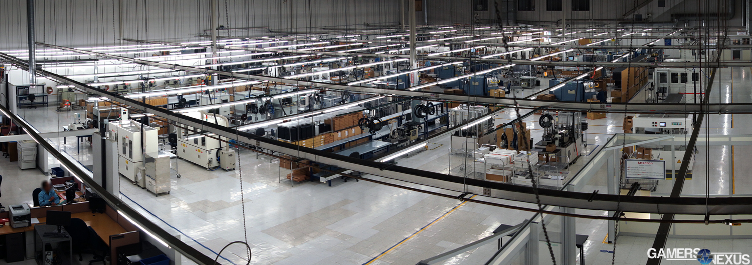
We recently visited Kingston Technologies' headquarters in Fountain Valley, CA, where we were able to tour on-site production facilities and talk about RAM & SSD assembly. Most of our time was spent exploring labs and wandering through the aisles of SMT lines, finally concluding with a trip to the shipping robotics and packaging room. This article and accompanying video give an insider walkthrough of SMT lines and the memory testing & assembly process, providing a bit of insight as to "how it's made."
Anyone producing board-mounted hardware (memory, motherboards, video cards) is using SMT lines (Surface-Mount Technology) at some point in the process. SMT lines use largely standardized, industry-wide machinery to assemble a product, solder components to it, electrically test the product, and eventually spit out the unit for shipping and/or further testing. Because SMT lines are standardized, they can be configured to produce multiple types of products -- the same lines that produce RAM can also be used for motherboards (though are configured differently).
Kingston Senior Technology Manager Mark Tekunoff gave us a walkthrough of the SMT lines and packaging machinery in their Fountain Valley, California facilities; the SMT lines weren't in operation when we were there, unfortunately, but we still show the equipment and Tekunoff explains how it all works. The packaging robotics (toward the end of the video) are in full operation and are quite cool to see in action, so definitely check those out.
As an aside, you may find our previous collaborative effort with Kingston/LSI of interest, which explains the design-dev-test-fab lifecycle of an SSD.
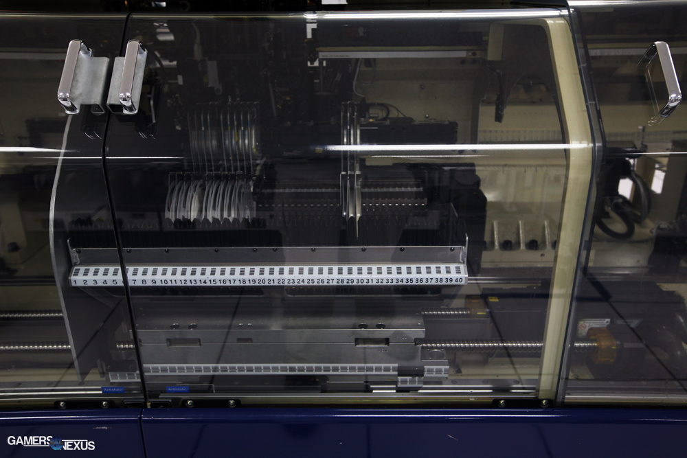
Tekunoff does a solid job at explaining the SMT process, but to reiterate: SMT lines are composed of a string of machines (in a line - big surprise) with conveyor belts that move the product through the assembly process. A stencil is used (shown in the video) to guide the solder placement; after the initial layer of solder paste is applied to the PCB, the boards are moved via conveyor belt into an optical inspection machine (for quality) that examines solder paste application using a laser.
If the inspection passes, the PCBs are passed through to a Pick & Place machine that places on-module components (caps, resistors). Next, DRAM is placed onto the modules -- this is the point where the product starts to resemble something we're all familiar with. During component-placement, boards are held stable by a dual-vacuum nozzle, which applies pressure to prevent movement while components are positioned. With all the components mounted on the board, we then follow the product to the reflow machine (effectively a large oven), which melts the solder (~255C) and attaches the components to the PCBs. If you've ever had to reflow a laptop GPU in your oven, it's largely the same process - just bigger and a good deal hotter.
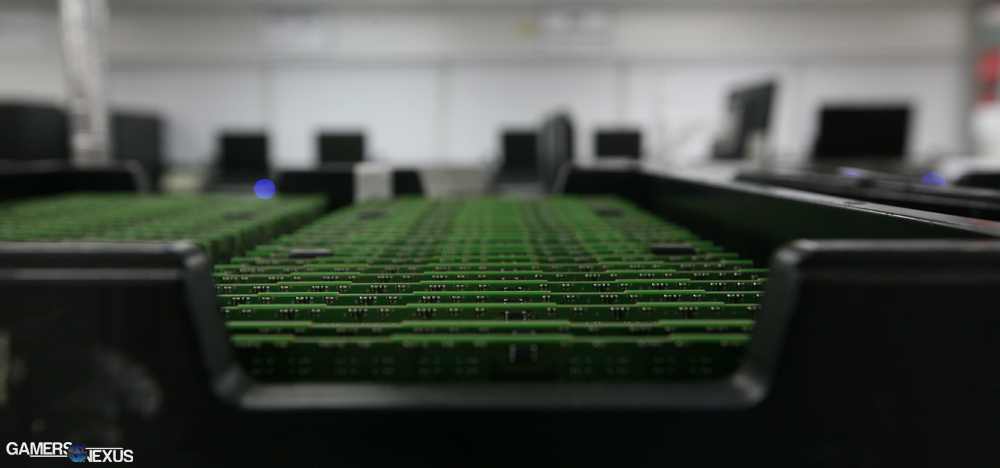
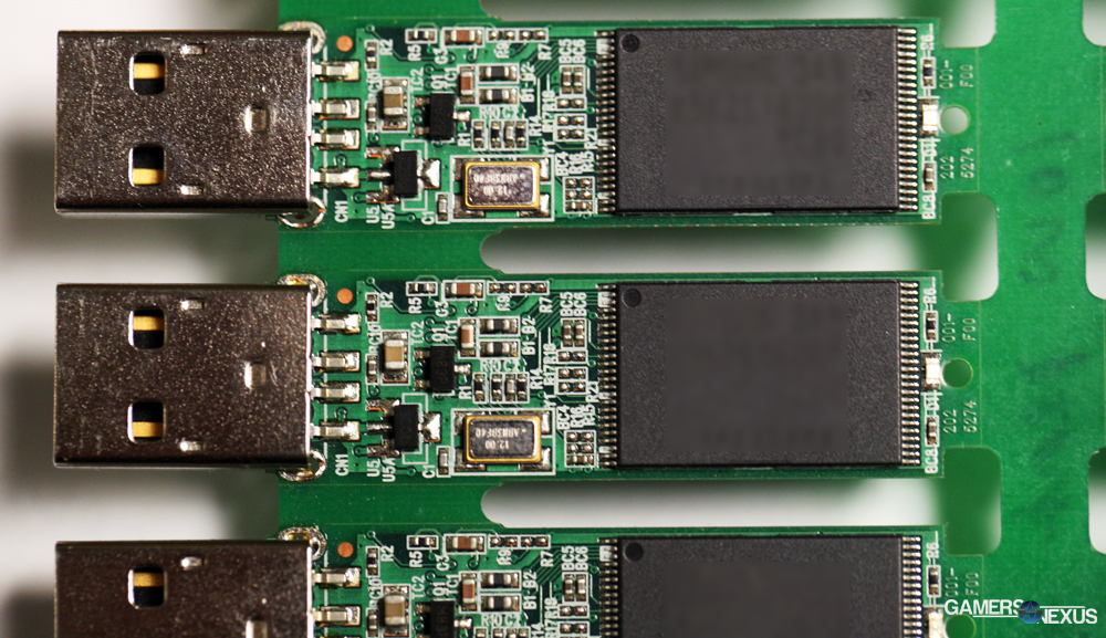 This is what a "batch" of USB keys looks like prior to being chiseled out and enclosed. This is what a "batch" of USB keys looks like prior to being chiseled out and enclosed. | 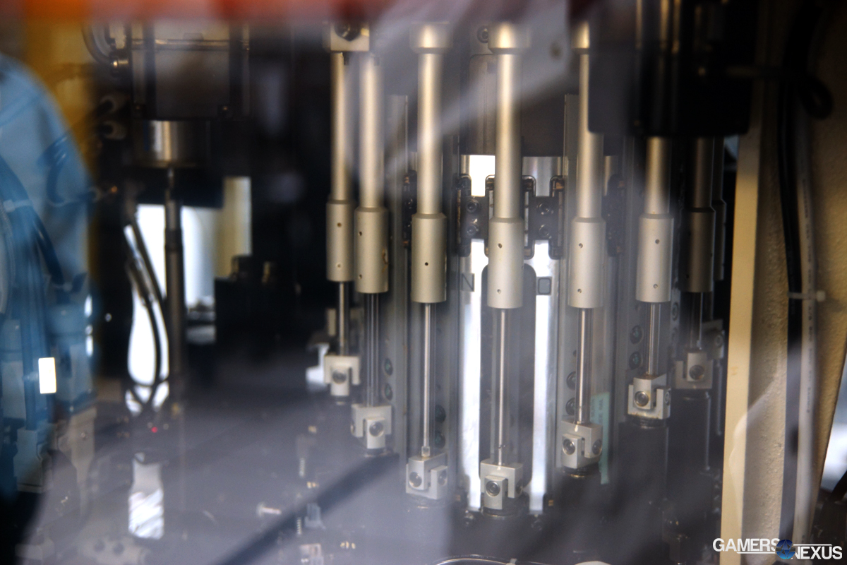 A Pick & Place Machine uses suction pressure to mount small components to boards. A Pick & Place Machine uses suction pressure to mount small components to boards. |
 |  The rear of the above Pick & Place machine, where caps/resistors/etc are found in the tape reel. The rear of the above Pick & Place machine, where caps/resistors/etc are found in the tape reel. |
Further optical inspection and testing is performed by machines prior to the modules being labeled. To put the speed and accuracy of this task into perspective, industry-standard AOI (Automated Optical Inspection) equipment like Kingston's can process approximately 3000-5000 tasks per minute, depending on the job at hand. Once the devices (again) pass automated optical inspection and they're labeled, a final machine cuts modules out of their palette (think of how you'd pop plastic pieces out of a mold for a model car -- now imagine doing it with a massive Dremel). The devices are then sent to be tested, packed, and shipped.
How long does it take to make a stick of RAM?
Out of curiosity, I asked Kingston PR Rep Danny Ordway for the approximate time-to-completion for a memory module. Though the company hasn't officially timed the process, here's what we were told:
It would take a one-sided memory module 15 to 30 minutes to get through the SMT line (in a perfect world). Double this time for two-sided modules. It would take about 4 hours to get out the door. This includes packaging and testing. This is considering everyone throughout the process dropped everything else they were doing and just worked on this one memory module to get this out the door as fast as they can.
During our realistic process we do batches of 5k to 10k modules at a time - the process starts with a quality check, then the SMT line. There is a quality step at the beginning, middle, and end of the process. There are checks and balances throughout the entire process as it goes to different departments like QA, testing, and finished goods. We are big on testing and making sure the product works perfectly when it leaves our warehouse. This entire process takes about 4-to-6 days from start to getting the module out the door.
Aside from the time required to complete a module, a couple of other cool items are worth highlighting -- like some specific testing and assembly equipment.
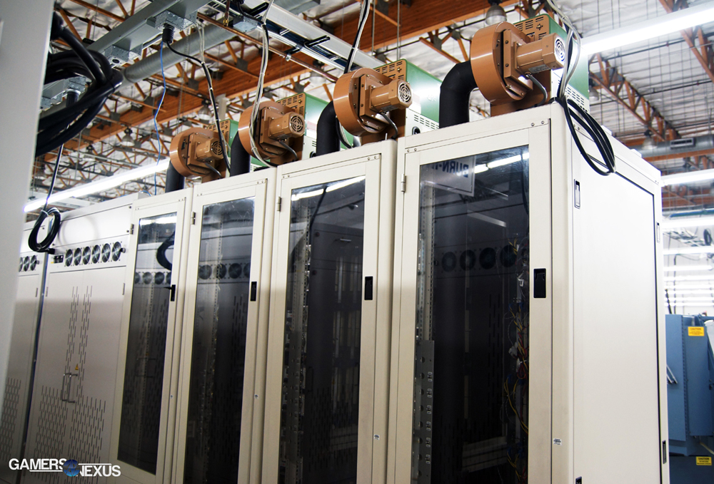
This is one of Kingston's thermal testing chambers, where heat is generated to test modules for stability (mostly server modules) under intense thermal situations. When GN photographer James Vincent pointed out the large blowers on top of the units, our Kingston tour guide mentioned that they discovered the blowers were actually unnecessary: The heat generated by hundreds of memory modules being simultaneously tested was enough for the thermal diagnostics.
Here's another:

Kingston's VP of Test Engineering designed this rig, internally known as the KT2501. This fully-automated bench is tasked with spot-checking memory compatibility with motherboards as they're rotated through the system. Motherboards are moved through the line on a conveyor belt, where automated "arms" outfit the sockets with in-test memory modules. Each specific board / RAM configuration is tested, marked as a pass or fail, and then the memory modules are uninstalled by the same machine. The KT2501 is rated to test up to 60 motherboards simultaneously.
And another:

This is one of the final machines to touch the product before it's shipped, responsible for the final boxing of the product (you can see this in action around ~5:00 in the video). Suction pressure is applied to the product (like an SD card) to shift it from the palette (received from manufacturing plants in Asia) to a conveyor belt, which eventually has the product placed into retail or bulk packaging.
Despite all the automation technology, Kingston still employs individuals who pack small and specific orders. For instance, if a client has a need for 25 specific module kits for regression work, it'd be quicker to hand-pack that shipment than configure the machine for the order.
GN writer Patrick Stone pointed out plastic consumption while walking between boxes of retail packages, and Kingston was quick to note that they work very closely with some businesses on green initiatives. Some retailers -- like Amazon, as a well-known example -- request products to be delivered in smaller packages and with more condensed contents; because the product won't ever be displayed on a shelf, but instead shipped to the customer's door, there's no need for a larger 'hanger' package. As a sort of fun side note, one of the hurdles in the process of reducing plastic packaging was finding a means to automate instruction booklet folding to fit into an evermore condensed box.
Here's a final look at some of Kingston's test & assembly setup. mostly because the sheer amount of hardware is gleefully entertaining:

Racks-upon-racks-upon-racks of motherboards are used for memory testing (regression, compatibility, stability), theoretically weeding-out defective products before they make it out the door. Kingston has benches established for both enterprise- and consumer-specific testing.
That's it for this one -- check back soon for full coverage on nVidia's Silicon Failure Analysis lab, where we were able to film an inside walkthrough of multimillion dollar analytical equipment. And fly TEGRA-controlled drones into things. Oops.
- Steve "Lelldorianx" Burke.