NVidia’s Volta GV100 GPU and Tesla V100 Accelerator were revealed yesterday, delivering on a 2015 promise of Volta arrival by 2018. The initial DGX servers will ship by 3Q17, containing multiple V100 Accelerator cards at a cost of $150,000, with individual units priced at $18,000. These devices are obviously for enterprise, machine learning, and compute applications, but will inevitably work their way into gaming through subsequent V102 (or equivalent) chips. This is similar to the GP100 launch, where we get the Accelerator server-class card prior to consumer availability, which ultimately helps consumers by recuperating some of the initial R&D cost through major B2B sales.
Aside from the obvious B2B target, which always means a higher cost, the V100 GPUs detailed at GTC run a die size of 815mm^2 – the largest we’ve seen anytime recently, with the P100’s already-large 610mm^2 towered over by the V100. Greater die size means lower yield, with more of the wafer thrown out per dice, and so cost goes up with that lowered yield.
Volta is brand new: This is not a Kepler-, Maxwell-, or Pascal-based architecture that “only” features efficiency optimizations; rather, Volta institutes a new type of core for deep learning applications (the “Tensor core,”) and builds ground-up a new GPU. Some organization and clustering remains the same on the block diagram – like SMs, which still contain 64 CUDA cores per Accelerator-class SM – but updates have been made to thread execution that haven’t yet been fully detailed.
This is not a consumer product, but just like the P100 GPU (deep-dive here), it’ll eventually make its way down to consumer-level devices. The major change with V100 is its introduction of tensor cores, something which will likely be entirely useless to consumers, but are critical to business operations.
Let’s start with an overview of the block diagram:
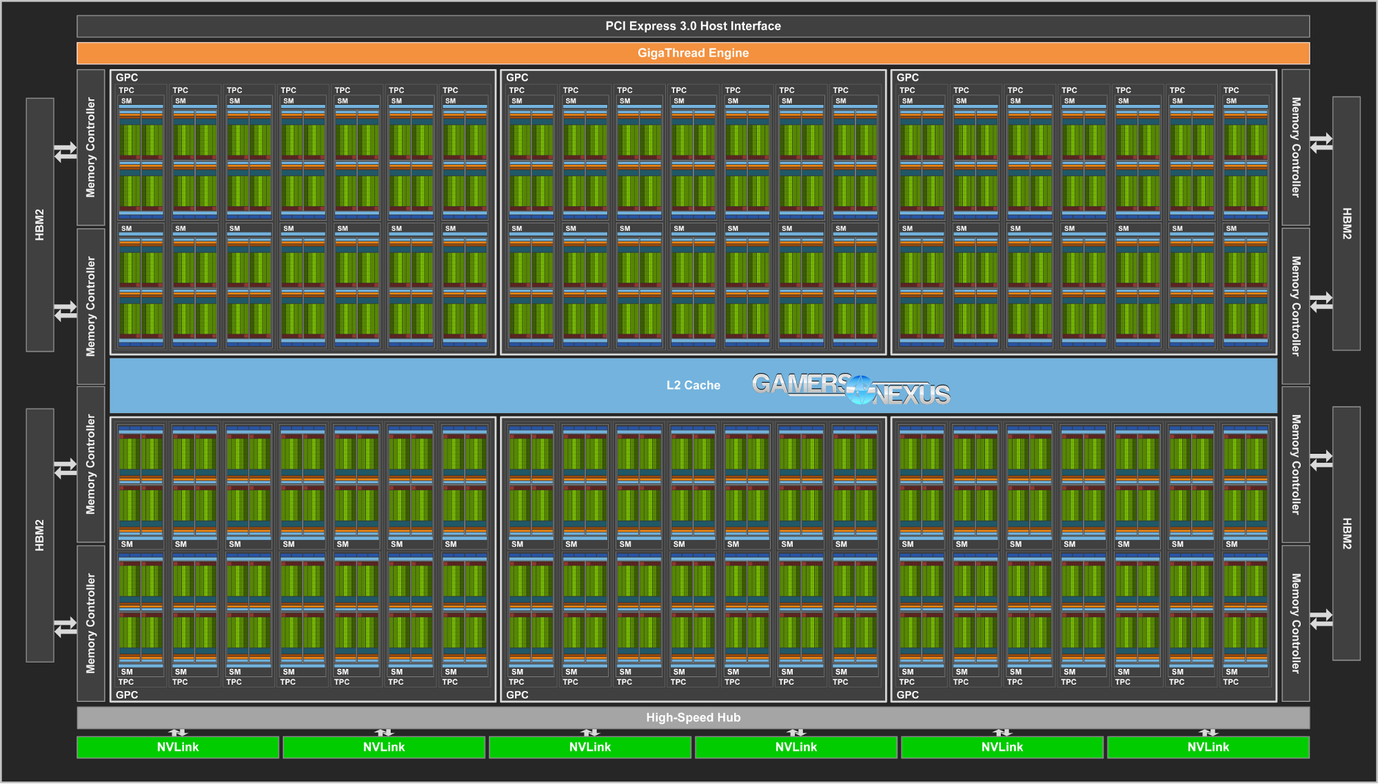
This is the full-size V100 block diagram, as built atop one of the largest pieces of silicon we’ve seen on a GPU. The die size for V100 is 815mm^2, around 30% larger than P100’s 610mm^2. For comparison, consumer-grade 1080 Ti GP102 chips are 471mm^2.
Full V100 hosts 5376 FP32 CUDA cores across 84 SMs, using similar organizational hierarchy to GP100 at 64 cores per SM, with a 1:2 FP64 ratio and 2:1 FP16 ratio. The result is 15TFLOPS of single-precision compute, about 8TFLOPS of double-precision, and about 30TFLOPS of FP16. For deep-learning, FP16 is useful as the precision is not needed when working with such large data matrices. Despite similar organizational layout to P100, the actual architecture is vastly different. Scheduling and thread execution have been reinvented on V100, something for which we don’t yet have full details, and the introduction of Tensor cores complicates things.
Alongside the 5376 CUDA cores are 672 Tensor cores, with each SM holding 8 Tensor cores. A Tensor core is targeted for HPC, deep-learning, and neural net computations, clustering ALUs into a single unit that specializes in fuse-multiply-add operations across two 4x4 matrices. Each Tensor core can execute 64 fuse-multiply-add ops per clock, which roughly quadruples the CUDA core FLOPS per clock per core. For large dataset COMPUTE work, this is a big deal.
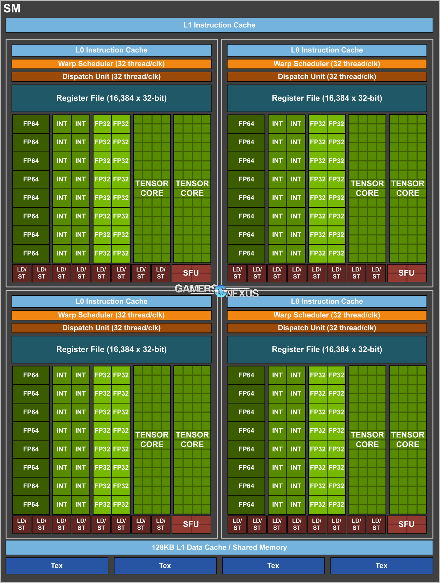
Here’s a shot of the SM layout. Each SM contains two TPCs that contain blocks of FP64, FP32, INT, and Tensor core units. This is just a block diagram and not necessarily representative of actual die space allocation to the Tensor cores, but it’s looking like a large part of V100 is allocated to this new core type.
The usual four TMUs are present on each SM, totaling 336 TMUs across 84 SMs to P100’s 240TMUs across 60SMs. These are indicated by the “tex” marks on the board.
The Volta architecture will be built on a new 12nm FinFET process from TSMC and, at 815mm^2 with 21.1B transistors, it’s bumping against the reticle limit of TSMC’s manufacturing technology.
Pricing looks to be about $18,000 per unit, which is high because of the yield concerns for such a large die. Yields will inherently be lower with bigger chips, which increases manufacturing cost – but big COMPUTE centers will readily invest the money. Initial Tesla GV100 Accelerators will be a cut-down version of the V100 die, hosting 5120 cores rather than 5276.
HBM2 is present on GV100 just like on the GP100, and in the same layout: four stacks total of HBM2, totaling 16GB capacity on a 4096-bit bus. At this time, this is the limit of HBM2 without increasing stack count.
Consumer products are targeted for 2018, as has been the case since nVidia revealed its roadmap in 2015.
Editorial: Steve Burke
Video: Andrew Coleman