Intel has enjoyed relatively unchallenged occupancy of the enthusiast CPU market for several years now. If you mark the FX-8350 as the last major play prior to subsequent refreshes (like the FX-8370), that marks the last major AMD CPU launch as 2012. Of course, later launches in the FX-9000 series and FX-8000 series updates have been made, but there has not been an architectural push since the Bulldozer/Piledriver/Steamroller series.
AMD Ryzen, then, has understandably generated an impregnable wall of excitement from the enthusiast community. This is AMD’s chance to recover a market it once dominated, back in the Athlon x64 days, and reestablish itself in a position that minimally targets parity in price to performance. That’s all AMD needs: Parity. Or close to it, anyway, while maintaining comparable pricing to Intel. With Intel’s stranglehold lasting as long as it has, builders are ready to support an alternative in the market. It’s nice to claim “best” on some charts, like AMD has done with Cinebench, but AMD doesn’t have to win: they have to tie. The momentum to shift is there.
Even RTG competitor nVidia will benefit from this upgrade cycle. That’s not something you hear a lot – nVidia wanting AMD to do well with a launch – but here, it makes sense. A dump of new systems into the ecosystem means everyone experiences revenue growth. People need to buy new GPUs, new cases, new coolers, and new RAM to accompany any moves to Ryzen. Misalignment of Vega and Ryzen make sense in the sense of not smothering one announcement with the other, but does mean that AMD is now rapidly moving toward Vega’s launch. Those R7 CPUs don’t necessarily fit best with an RX 480; it’s a fine card, just not something you stick with a $400-$500 CPU. Two major launches in short order, then, one of which potentially drives system refreshes.
AMD must feel the weight borne by Atlas at this moment.
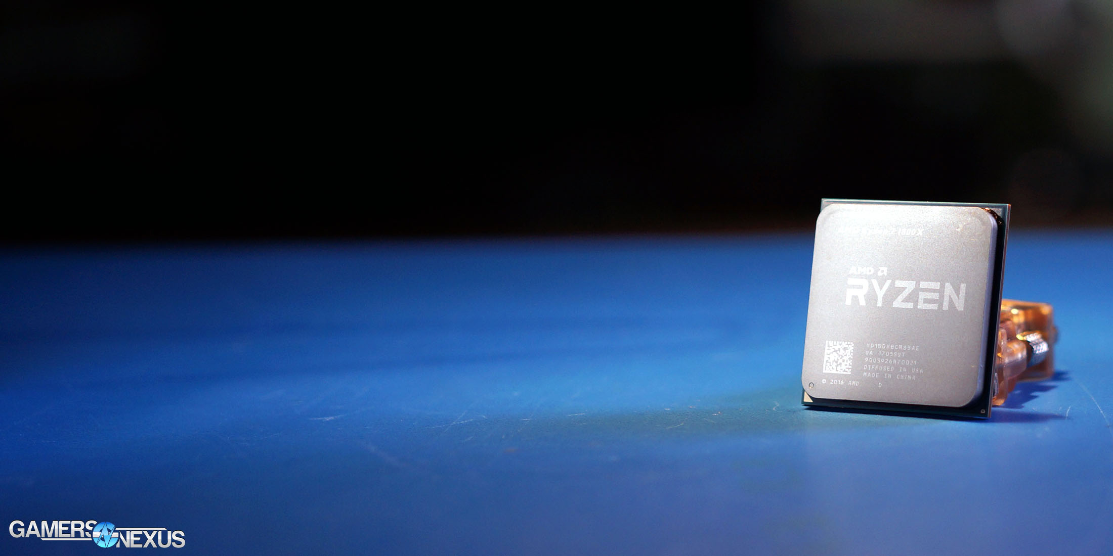
In this ~11,000 word review of AMD’s Ryzen R7 1800X, we’ll look at FPS benchmarking, Premiere & Blender workloads, thermals and voltage, and logistical challenges. (Update: 1700 review here).
AMD Ryzen R7 1800X vs. 1700, 1700X Specs
| Ryzen R7 1700 | Ryzen R7 1700X | Ryzen R7 1800X | Ryzen R5 1600X | Ryzen R5 1500X | |
| Socket Type | AM4 | AM4 | AM4 | AM4 | AM4 |
| Cores/Threads | 8C/16T | 8C/16T | 8C/16T | 6C/12T | 4C/8T |
| Base / Boost | 3.0GHz / 3.7GHz | 3.4GHz / 3.8GHz | 3.6GHz / 4.0GHz | 3.6GHz / 4.0GHz | 3.5GHz / 3.7GHz |
| TDP | 65W | 95W | 95W | ? | ? |
| Stock Cooler | Wraith Stealth (65W) ~28dBA | Wraith Spire (95W) ~32dBA | Wraith MAX (125W) ~38dBA | ? | ? |
| Memory Support | 2ch/2rank: 1866-2133 2ch/1rank: 2133-2400 1ch/2rank: 2400-2667 1ch/1rank: 2667 | 2ch/2rank: 1866-2133 2ch/1rank: 2133-2400 1ch/2rank: 2400-2667 1ch/1rank: 2667 | 2ch/2rank: 1866-2133 2ch/1rank: 2133-2400 1ch/2rank: 2400-2667 1ch/1rank: 2667 | ? | ? |
| Release Date | March 2 | 3/2/17 | 3/2/17 | 2Q17 | 2Q17 |
| Price | $330 | $400 | $500 | Sub-$300 | Sub-$300 |
Ryzen debuts strictly with the R7 series of CPUs, leaving subsequent R5 and R3 CPU launches to later dates. The R5 1600X and R5 1500X will both ship sub-$300, from what AMD tells us, and should begin availability sometime in 2Q17. The R3 budget CPUs won’t arrive until 2H17.
For today, we’re strictly focusing on the R7 1800X ($500). We had just under a week to benchmark the R7 1800X between touching down post-event and taking off for the GTX 1080 Ti announcement, but we do have the R7 1700 and R7 1700X available for testing. Our R7 1700 review, if all goes as planned, will publish tomorrow. We hope to follow this up immediately with the R7 1700X, barring any unforeseen issues during testing – and there have been many thus far. See pages 2 & 3 for that discussion.
At time of publication, the R7 1800X will be available for $500, the R7 1700X for $400, and the R7 1700 for $330. We did not receive stock coolers with any of our test units, but have acquired some and will receive them shortly.
Interestingly, AMD explicitly indicated that Zen will offer “near perfect scalability” across multiple sockets and multiple dies. This statement was more targeted at server, where you might have a dual-socket motherboard, but we’ll go on record now as predicting an eventual dual-die package under the Zen architecture. Any such chip would almost certainly not make it to the gaming market, and we don’t cover server/enterprise.
Let’s talk architecture.
AMD Zen Architecture (“Ryzen” CPUs)
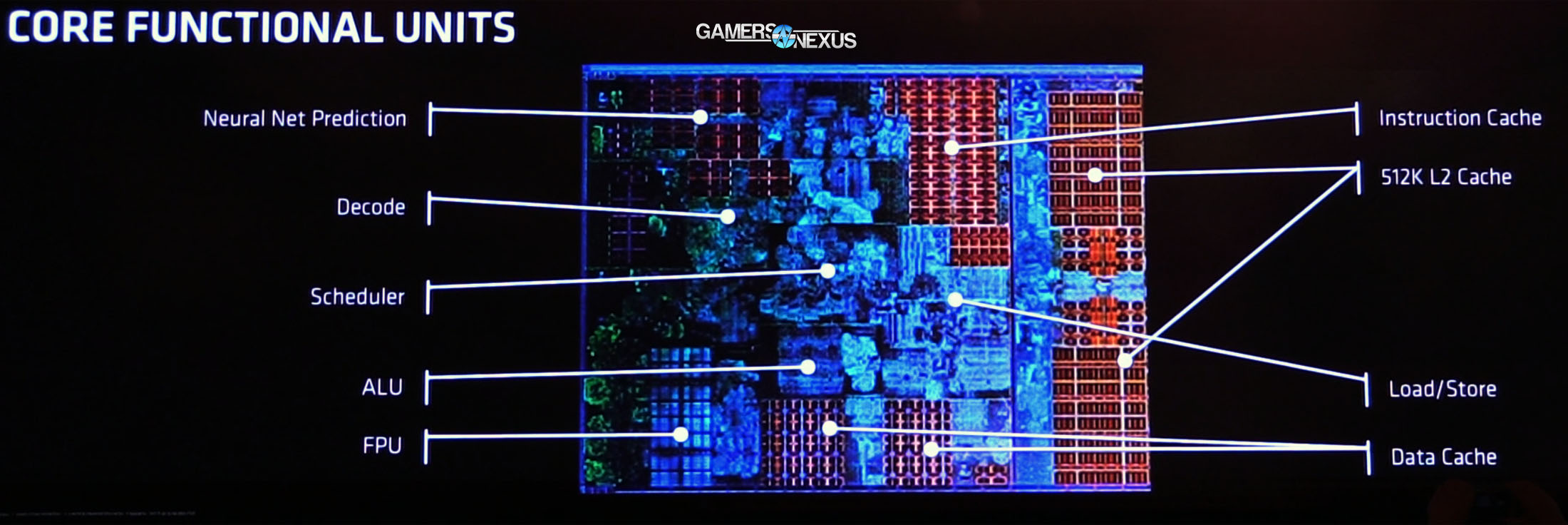
The R7 desktop CPUs are all built on 8C/16T designs, using two of AMD’s new CCX modules as a replacement to the Bulldozer architecture. The Zen CCX moves to a single FPU per core, away from the 1FPU/2INT unit design of Bulldozer. Each CCX is a 4C/8T module, resulting in two modules for the R7 CPUs (2x CCX = 8C/16T). Devices that operate on 4C/8T will use a single CCX on the die. This also means that we almost certainly will not see dual-core Zen architecture desktop CPUs based on the current design, unless AMD goes the route of disabling units on the package. This same architecture is shared across desktop/enthusiast, server (see: Naples), and the forthcoming laptop variants of Ryzen CPUs. As an aside, there are presently no portable Zen processors – but AMD does have plans to move this direction.
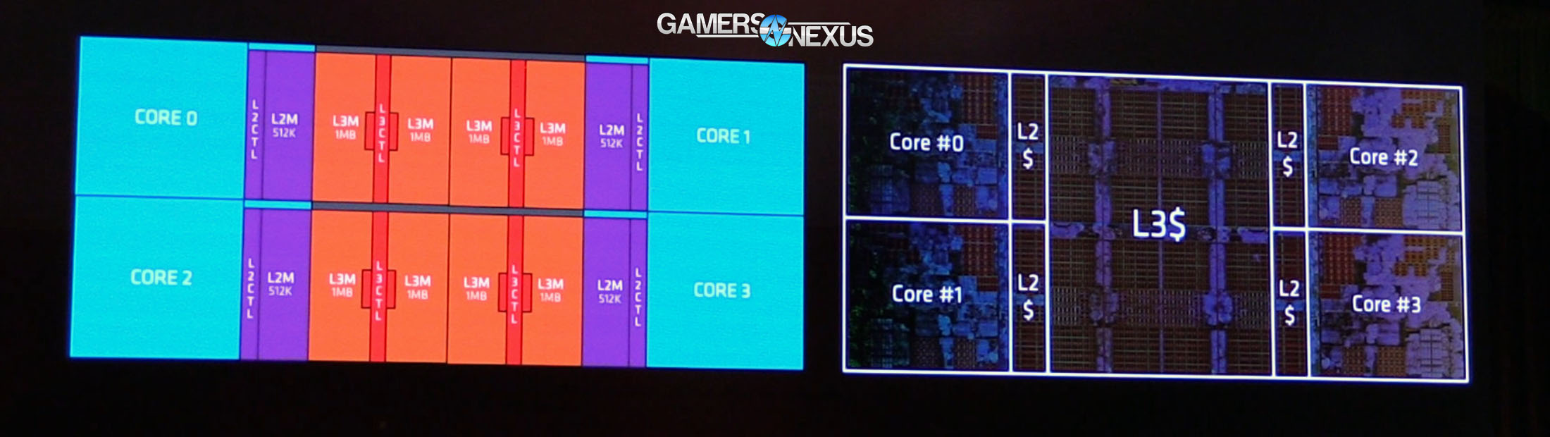
Each CCX is connected to its own L3 Cache, with L2 privatized on a per-core level. Each pairing of two threads will split resources between the L2 Cache, a SIMD (Single Instruction, Multiple Data), and FPU, but we understand that there will be no cross-contamination between cores of these resources. AMD is running 512K of L2 cache per core, at 1.5mm^2 per core. This 512K cache is 8-way associative, so AMD doesn’t need probes to interfere with low-latency caches during snoops. Avoiding snoops on faster caches prevents long latencies that can damage performance. L3 Cache totals 8MB at 16mm^2 of the total die area (44mm^2), is 16-way associative, and shares PLL with all the cores. The L3 cache can be shut down if only L1 and L2 are in use, serving as a power saving feature during periods of zero L3 cache hits. Keep in mind that this is something that happens without user intervention or knowledge – there’s no switch you throw.
Each core is able to access 32KB L1, 512K L2 (cache per core), and 8MB L3 (per CCX) with the same latency, thanks to the CCX’s intentionally compartmentalized layout. Alongside other optimizations made, like a new prefetcher for L1 and L2 data, AMD advertises an approximate 2x increase in L1 and L2 bandwidth, or about a 5x increase in L3 bandwidth over previous generations.
Zen’s Victim Cache will match the fastest core on the CCX. L3 will follow this core’s trajectory as it downclocks (e.g. when load dies down), permitting some power savings without sacrificing the ability of the cache to keep up with faster cores. Here’s a closer look at the L3 Cache:
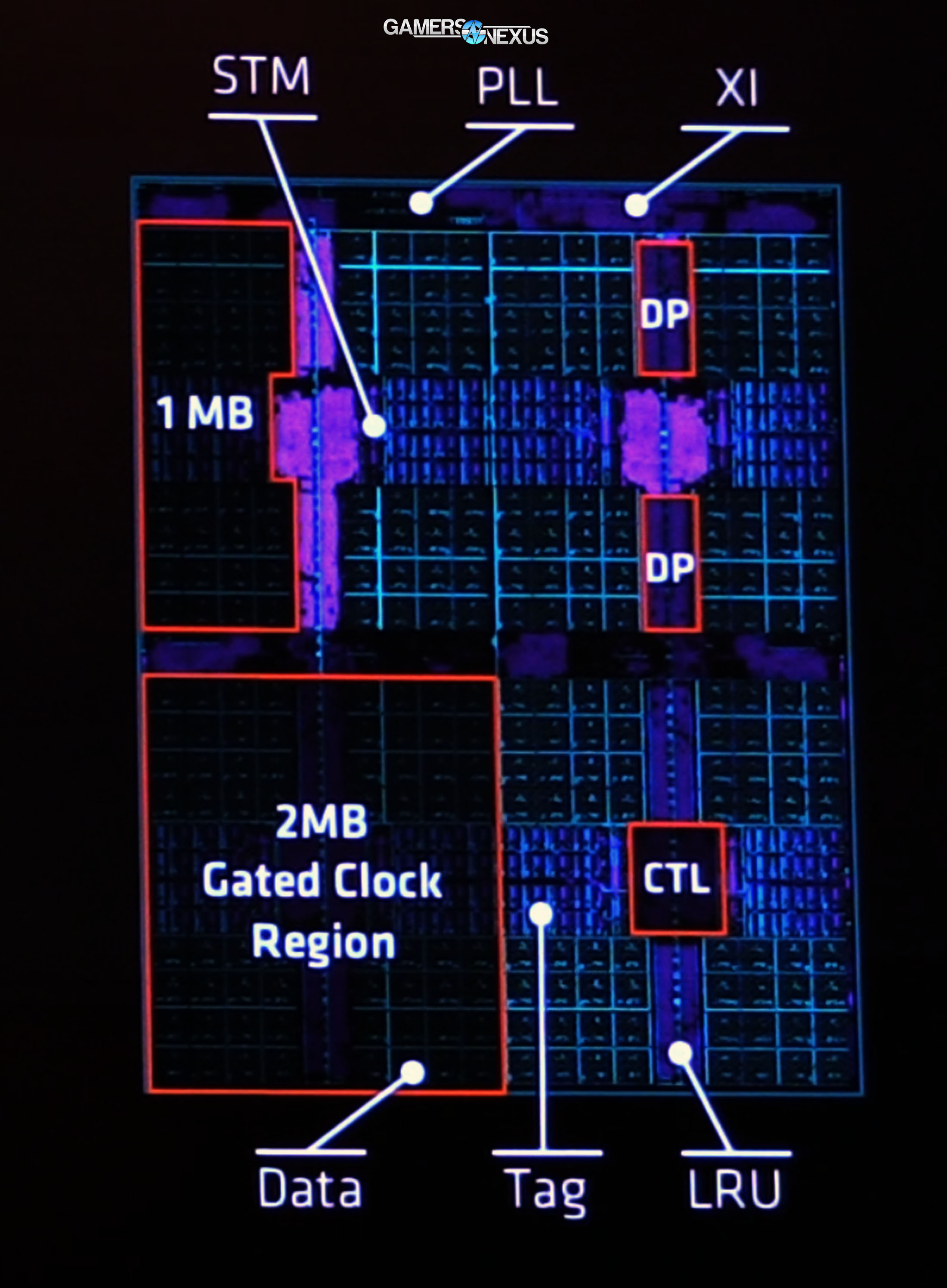
Above: L3 Cache
A 2MB gated clock region is positioned in the bottom-left of the L3 block diagram. Aggressive clock gating is performed as a power savings measure, but frequency matching and sensors scattered across the chip should ensure minimum performance loss for these reductions. All tradeoffs for power are calculated, allowing more efficient utilization of the total power budget for the chip.
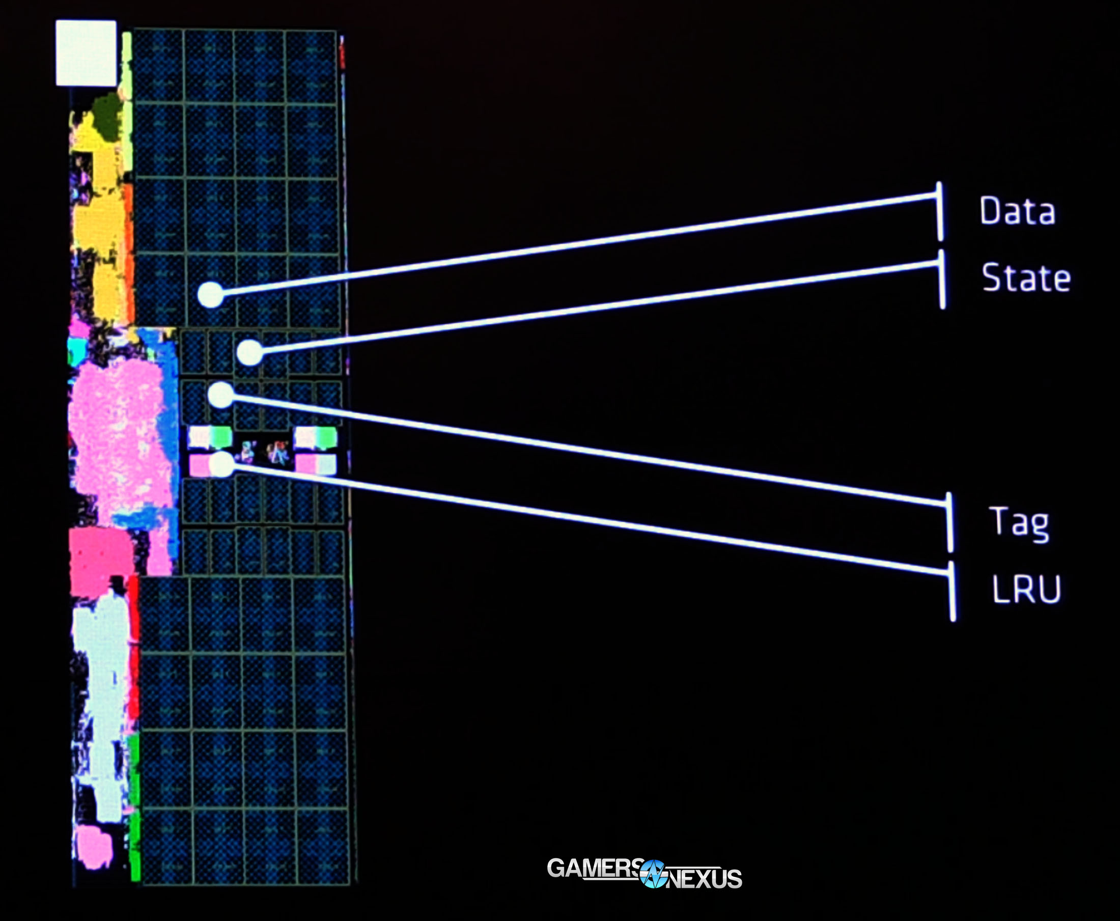
The static RAM cells are less dense than Intel’s mature fabrication, but AMD still boasts improvements. AMD is using six-transistor SRAM for tag and data, with eight-transistor SRAM for state.
AMD’s L1 cache has also now been switched over to a writeback L1 Cache and off of the previous writethrough design. We have an interview with AMD Chief Architect Mike Clarke going live this week (check here), which will grant a cursory look at the implications of this change. For now, here’s an excerpt:
“On the writethrough cache, your writes would both go into the L1, and then they would be propagated again to go into the L2. With the writeback cache, the writes go into the L1 cache, and they don’t go into the L2 and the states maintain in the L1. They may transfer to the L2 once they’re evicted from the cache, but they’re not kept updated in both places […] not moving the data ‘til you absolutely have to.
“The shadow tags were a nice optimization. We have a victim cache for our L3, and so when a core misses in its L2, it might miss in the L3, but it might be in another L2 cache local in the core. Typically, we would just probe all those to find it. That causes some performance problems with bandwidth in the L2 and burns a lot of power; instead, we built the Shadow Tags within the L3 Macro, and that lets us quickly know which one of the cores the data is in and go get it. We also did it in a unique two-stage mechanism. With a partial lookup, we can know whether we’re going to hit or not, and only fire the second stage if we hit on the first stage. That lets us save about 75% of power than an equivalent implementation where you’d probe everywhere]. It’s pretty amazing.”
There’s also a new uOp-cache, which Clarke details as:
“One of the hardest problems in trying to build a high-frequency x86 processor is that the instructions are actually of variable length. That means to try to get a lot of them to dispatch in a wide form, it’s a serial process. To do that, generally we’ve had to build deep pipelines -- very power-hungry to do that.
“We call it an op-cache because it stores them in a more dense format than the past. Having seen them once, we store them in this op-cache with those boundaries removed, so when you find the first [instruction], you find all its neighbors with it. We can actually put them in that cache eight at a time, so we can pull eight out per cycle. We can cut two stages off that pipeline of trying to figure out the instructions. It gives us that double-whammy of a power savings and a huge performance uplift.”
AMD Zen Core
On a per-core level, the biggest item of note is that AMD’s move to integrate SMT (simultaneous multithreading) results in two threads per core. This can be thought of as similar in concept to Intel’s Hyperthreading, though the two are executed in different ways. Developer implementation of each approach to SMT will require fine-tuning as Ryzen ships and matures.
The uOp queue is fed 4 instructions/cycle from decode, then sent down the pipe to AMD’s segmented integer and floating point units. Within Integer land, the rename space is fitted with 168 registers, and can handle 192 in-flight instructions. We also see four ALUs and two AGUs per INT block within the core, eventually feeding down to 2 L/S units capable of 2 loads and a store per cycle. Zen’s 2x AGUs (versus the 3x AGU layout of competing Intel arch) further aids in power savings, though with some specific workload limitations that would not be present on Skylake. That said, the decision should help AMD’s clocks, and the company clearly believes the trade-off to be worthwhile. David Kanter has an excellent piece further discussing Zen architecture and its decisions as contrasted to Skylake/Haswell, and can be read in the Microprocessor Report from August, 2016.
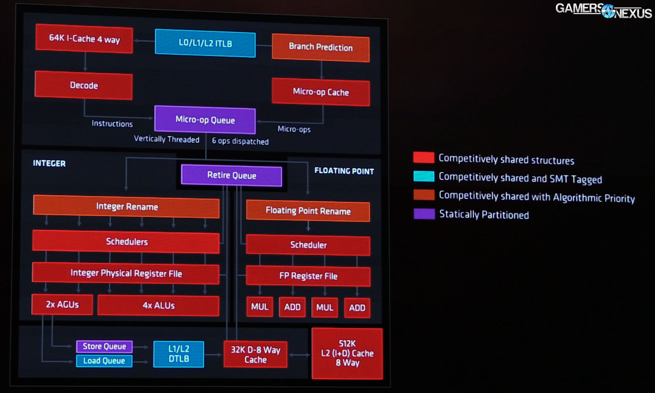
This design, coupled with AMD’s decision to defer to 2x 128-bit wide AVX units (versus Skylake’s 256-bit wide option), mean that less die space is consumed for the core. If you were wondering about AMD’s 44mm^2 vs. 49mm^2 metrics, these decision are part of that.
Loads are now faster to the FPU, taking 7 cycles instead of 9 on previous architectures. The floating point block of the core is outfitted with 2x MUL and 2x ADD, with Zen now capable of performing fused multiply-adds. Fused Multiply-Adds reduce rounding to a single execution, rather than two roundings for the add and then the multiply (e.g. x*y+z will only be rounded once with FMA). This isn’t new, but it’s new to Zen. Alongside other instruction types, advanced vector support includes AVX2 and AVX512 on AMD’s Zen architecture, new in the time since Bulldozer. Blender, the 3D animation and rendering software, supports AVX2 in render engine cycles, for a real-world use case. Prime95 also uses AVX.
Power Delivery
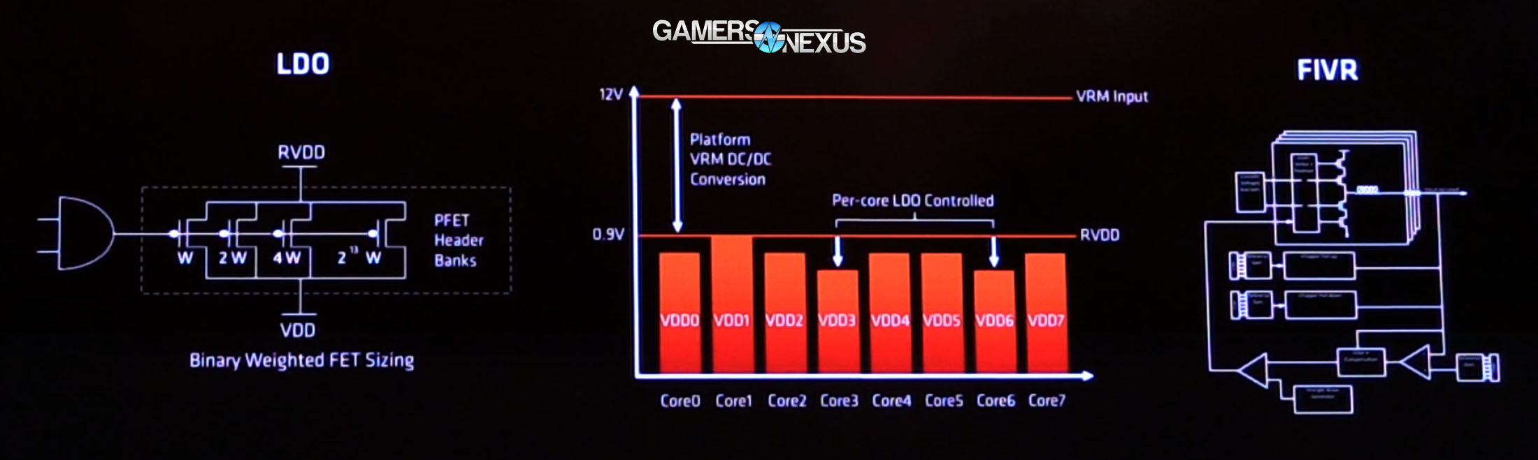
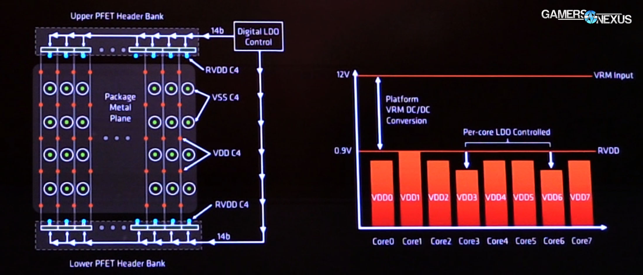
AMD’s opting out of FIVR, the fully-integrated voltage regulator that Intel has recently used. Instead, AMD is opting for a more traditional linear voltage regulator and LDO (low-dropout regulator), and is localizing voltage regulators across the core. Continuing its newfound obsession with sensors (for the record, we think this is a good thing), AMD has 9 vDroop detectors alongside 48 power supply monitors that help ensure stable and fine-tuned voltage regulation. When asked the benefit of LDOs, we were told that an LDO allows for faster cores to operate with lower voltage, thus saving power (and heat).
Adaptive voltage and frequency scaling (AVFS) also makes an appearance here, with Zen supporting 25MHz granularity of the clock as it attempts to reach boost states. This sees play in several ways and is comparable in concept to recent Polaris and Pascal posts we’ve made regarding boost features. Although power and heat may seem boring from an enthusiast user’s standpoint, the two are closely related to a chip’s overall performance. It is not possible to clock high if heat is a concern, and heat is usually a concern because power draw is a concern. The two are interwoven.
Boosting technologies allow for rapid regulation of frequency versus load, voltage, and temperature. If the CPU runs along the maximum Junction temperature (TjMax = 75C), the CPU – just like a GPU – will downclock itself rapidly and in (hopefully) small increments. This will prevent a thermal runaway scenario wherein the chip and cooler can no longer hold temperature, eventually resulting in a thermal trip. This might be a thermal shutdown or severe downclocking, depending on EFI configuration. By downclocking, temperatures can be checked on an as-needed basis, but performance loss can be profound under extreme conditions.
This comes with an obvious performance detriment: The less stable the clock, the more hits to framerate (particularly frametimes, in our GPU thermal testing). The smaller increments implemented in AMD’s new architecture mean that clock stability should remain relatively flat in an over time chart.
If this interests you, we have a thermal, voltage, and power testing section of this review with more information.
AMD AM4 Chipset Comparison
| X370 | B350 | A320 | X300 | A/B300 | |
| USB 2.0 | 6 | 6 | 6 | 0 | 0 |
| USB 3.1 G1 | 6 | 2 | 2 | 0 | 0 |
| USB 3.1 G2 | 2 | 2 | 1 | 0 | 0 |
| SATA | 4 | 2 | 2 | 0 | 0 |
| SATA Express (2x SATA III or 2x PCIe 3.0) | 2 | 2 | 2 | 0 | 0 |
| PCI-e 2.x | 8 | 6 | 4 | 0 | 0 |
| SATA RAID | 0, 1, 10 | 0, 1, 10 | 0, 1, 10 | 0, 1 | 0, 1 |
| Multi-GPU | Yes x8/x8 or multiplexed | No | No | Yes | No |
| Overclocking | Yes (Requires better cooling) | Yes | No | Yes | No |
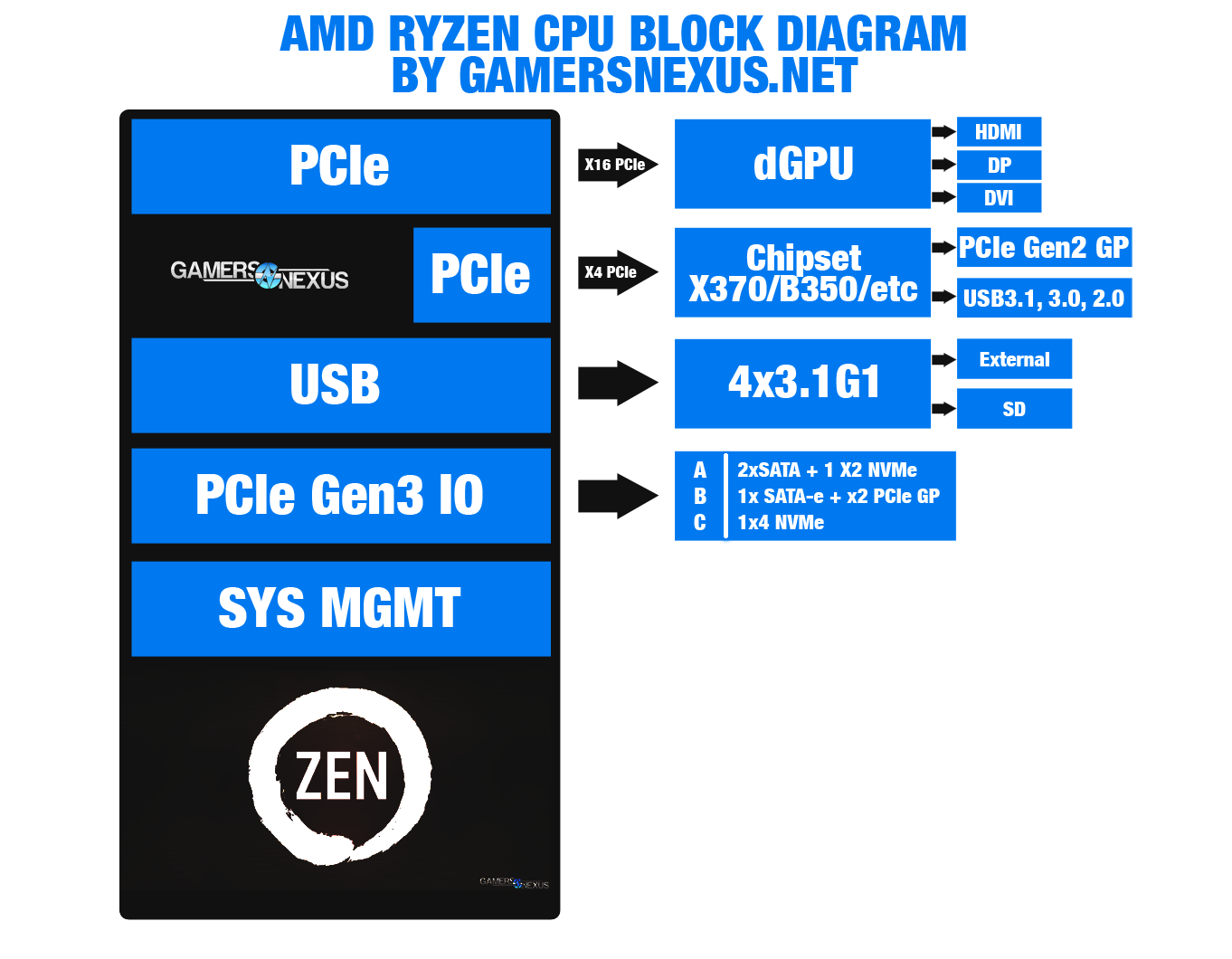
Here’s a block diagram that GN previously made to help explain Ryzen / Zen architecture:
To learn more about the AM4 chipset differences in depth, check our previous content piece: AM4 Chipset Comparison – X370, B350, A320, and A/B/X300.
Before moving into methodology and testing, we’ll address some of the internet’s pre-launch leak concerns regarding memory support and logistical challenges for Ryzen.
Continue to Page 2 to learn about memory support & logistical challenges.
Official AMD Ryzen Memory Support
Several sites and fora discussed potential memory limitations on Ryzen in the leaks leading to embargo lift. To some extent, these were true; that said, the internet went a little crazy with its claims on either side of the memory discussion, as it tends to do.
Ryzen officially supports ~2666MHz right now. This is straight from an AMD presentation at last week’s San Francisco event. Ryzen officially supports:
- Dual-channel, dual rank: 1866-2133
- Dual-channel / single rank: 2133-2400
- Single-channel / dual rank: 2400-2667
- Single-channel / single rank: 2667
AMD’s test documents sometimes suggest ~2666MHz speeds for memory during testing to ensure no miscommunication during handshakes with the memory controller, which could damage performance. We have also received suggestions to operate at higher frequencies if they are stable, depending on whom you ask.
We were able to clock up to 2933MHz and used this for most finalized testing. At time of testing, we did not observe performance improvements by moving from 2933MHz to 2666MHz. We were not able to sustain higher clocks than 2933MHz with the Corsair kit that we had access to, and there’s a lack of access to memory subtimings that further complicates higher clocks on DDR4. Now, that said, ASUS got its memory upwards of 3600MHz during the Editor’s Day. This can be done with memory training, presumably a memory kit from an ideal batch and with the right dies, and with fine-tuning of the settings. That includes reference clock modifications. To really get the most out of memory, you’ll have to manually tune reference clock (something we did not want to do for stock benchmarking tests), vDIMM, and then step through memory training, if present. This seems to be easiest on the ASUS Crosshair board that we used for review; in fact, of both boards that we have and in speaking with other editors, the ASUS Crosshair board seemed to offer the most complete feature set at time of early sampling.
To get memory functioning at higher frequencies, given the right motherboard and time, you could:
- Boot at 2400MHz
- Commit EFI change
- Boot at 2666MHz
- Commit EFI change
- Boot at 2933MHz
- Commit EFI change
- Configure vDimm to correct or slightly higher value (e.g. 1.4v)
- Boot to 3200MHz
If you are encountering a subtiming or kit validation issue, it is not possible to fix on the Ryzen platform at this time. No subtimings are accessible. There’s a good chance this stability also relates to memory ICs used, and note that memory vendors are ramping to validate new kits as we speak. Considering how strongly AMD suggested we avoid testing with kits which weren’t the one provided, we’d recommend potential buyers to check the supported CPUs list for memory kits.
Also during time of review, there was only one memory kit officially validated for Ryzen, and it’s the Corsair’s Vengeance LPX 3000MHz kit. Again, AMD and Corsair strongly suggested that we were not use other kits of memory for testing, and so this provided kit is the one used in our benchmarks. You’ll likely see that most other reviewers made the same decision. We were not able to sustain the higher advertised clock-rates of our better memory kits when using the AMD platform.
Ryzen’s Logistical Issues
Ryzen has had some logistical issues. AMD is stretched thin, as are partner samples, and we’re not the only people who’ve tried to get ahold of the team this week. Several manufacturers in the industry have indicated to GN the difficulty of obtaining retail samples for validation and media support, forcing us to get a little creative in our usual pings for sanity checks. Zen is a big push for AMD, and it was sprung on everyone with little notice; sure, we all knew it was coming, but the preparation period between final announcement and launch has been in the span of weeks to a month. AMD told GN in a last-minute phone discussion that most board vendors have had 3 weeks (from March 2) to finalize EFI, and noted that some motherboards still “need more time in the oven.” This should explain some of the initial bugs in EFI from multiple vendors. Note carefully that EFI version can heavily impact performance in some cases. GN used the latest (correct) ASUS EFI version, detailed on the next page, but other board vendors shipped updates late into the review week. Disparity in review performance can be partially attributed to motherboard support and EFI revision.
Board vendors aren’t the only ones who have had that limited window. That’s counting memory, cooling, and board partners alike.
Of all the architectures we’ve reviewed these past few years, Zen is the first one where we were receiving pings from manufacturing partners and system integrators to assist in sanity checks (third-party/peer data validation). Of course, we also sent several of these sanity check / validation requests to those same SIs and board partners (and have a 50-email long thread with AMD), along with several of our peers in the media space. Motherboard vendors have had limited time on EFI development, leaving most of the BIOS interfaces a little Spartan, and with at least one EFI update per vendor in the past week.
Cooling will be limited on day one, but should rapidly expand options. If you’re unhappy with the current selection of coolers, give it some time. Most of the brackets are on boats from China right now, or soon will be. Generally, any of the cooling manufacturers operating factories in China (due to long lead times) will be late to launch as a result of the scramble. Companies like Noctua and Alphacool, both of whom operate manufacturing outside of China, were able to get brackets or adapters turned around with a shorter lead time. That said, there are still other challenges.
In speaking with several cooling manufacturers, we’ve learned that AMD’s provided specification for cooler retention brackets is allegedly inadequate for usage by some cooler makers. This primarily affects makers of liquid coolers, which – by nature of their size and reduced sag – require less force than an air cooler might. According to the spec, from the information we’ve gathered, AMD is recommending 60-90lbft of force to secure an air cooler. There is allegedly no specification provided for smaller coolers, and so CLC makers are left taking their best guess at mounting force. The 60-90lbft number could result in excessive force, a problem for coolers which are not supported top-down on the pump head.
In speaking with these companies, it sounds like the delay on affected CLCs and AIOs will extend into mid-March. The manufacturers are planning AM4 brackets for existing product lines once they have been produced and shipped to channels.
Asked for comment, AMD stated:
“There are no specific guidelines for LCS/CLC – we do not differentiate between cooler types, but specify the minimum clamping force to ensure that during shipping or other transportation events that the CPU is held securely in the socket and maintain good contact.”
This said, some motherboards (like the ASUS Crosshair) support both AM3 and AM4 mounting holes. For these, you’ll need to separately grab an AM3 backplate, replace the AM4 backplate, and then mount your cooler normally. That is, assuming it’s one which doesn’t use a custom backplate (and those should still align with AM3 holes).
Where are the Mini-ITX Boards? (& EFI)
Board partner challenges were not limited to a small time window on EFI development. If you’re wondering where all the mini-ITX AM4 motherboards are, e.g. those with X300 chipsets, the answer is that most are still in design and development. Mini-ITX motherboards using the shrunken down AM4 chipsets have an extra layer of complexity – literally, generally needing an extra PCB layer – and that takes time to build. We’ve spoken with a few manufacturers and know that boards are on the way, they just might not all be here for launch.
For this launch, keep in mind that EFI version and motherboard will have an impact on performance in potentially large ways. Even smaller methodological things that we account for, like running Windows in “Performance” power mode rather than “Balanced,” can have sometimes noteworthy impact on performance. In this particular instance, it’s because of core parking.
Regardless, we’re trending into methodology discussion.
Continue to Page 3 for the test methodology.
CPU Test Methodology
Our usual testing methodology is defined further below, per typical copy/paste of methods between reviews, but we have a few explicit items to address with Ryzen.
During testing, GamersNexus discovered that Windows would occasionally engage core parking or other power saving features that could impact framerate in some games, specifically with Ryzen. This was not always detectable, but some games reacted more than others (our biggest observable difference was ~4-5%). As such, all tests were conducted in performance mode. We further discovered that SMT toggling improves performance in nearly all gaming use cases, and so tested with SMT both enabled and disabled. When asked about this, AMD supplied that it is likely on the ISV optimization side.
We’ve been using the newest (and correct) version of AMD’s chipset drivers since we began testing, and we’ve been on ASUS’ version 5704 (latest) BIOS for the Crosshair Hero VI. ASUS was good to provide us this update immediately when we reached out, though AMD officially distributed an older EFI version to reviewers; this older version is detrimental performance in some ways, as it was not the production-ready EFI. In speaking with other editors, MSI boards went through similar EFI updates that drastically changed performance, in some cases. A few toggles are broken in various EFIs we've looked at here, which can potentially skew results if the tester does not validate that the toggles work as advertised (performance modes, for instance, can toggle threads in some extreme cases). It is relatively easy to avoid unintentional corruption of test data so long as the tester rigorously validates thread count, clock-rate, and voltages prior to each major test sequence.
Fortunately, we had already retrieved the correct EFI from ASUS directly, and so did not have to test multiple EFI versions – though we did have to retest the platform and CPU multiple times for other validation. EFI version matters a lot in these very early days of Ryzen. This is an entirely new architecture – not some updated on a long-known design, like KBL was – and vendors were not prepared. Early EFI distributions were based on older uCode. Results will vary between test environments in greater ways than usual.
This part applies to all motherboards, CPUs, and platforms: For testing, we disable any performance bias options made available through EFI. ASUS often offers Cinebench or 3DMark performance bias configurations (boosting performance in specific applications). We disable these for fairness across platforms. All stock CPU options are left enabled for benchmarking, like Boost on Intel and AMD.
A clean image is used for all testing. We have Windows images on multiple SSDs, each labeled for the appropriate CPU architecture. We pull an SSD with the correct label from the shelf (e.g. Skylake, Broadwell-E, Ryzen) and use that for testing. Note also that Windows HPET can affect performance.
Because of how Ryzen’s boosting reacts to temperatures, we put the R7 1800X under the same liquid cooling we’ve used for all our major CPU reviews: the Kraken X62. This eliminates unpredictable thermal throttles during test.
Game Test Methodology
NVIDIA 376.33 drivers were used for all benchmarking. Game settings were manually controlled for the DUT. All games were run at presets defined in their respective charts. All other game settings are defined in respective game benchmarks, which we publish separately from GPU and CPU reviews. Our test courses, in the event manual testing is executed, are also uploaded within that content. This allows others to replicate our results by studying our bench courses.
Windows 10-64 was used for testing.
Each game was tested for 30 seconds in an identical scenario, then repeated three times for parity.
Average FPS, 1% low, and 0.1% low times are measured. We do not measure maximum or minimum FPS results as we consider these numbers to be pure outliers. Instead, we take an average of the lowest 1% of results (1% low) to show real-world, noticeable dips; we then take an average of the lowest 0.1% of results for severe spikes.
Core Components (Unchanging)
- NZXT 1200W Hale90v2
- For DDR4 platforms: Corsair Vengeance LPX 32GB 3200MHz*
- For Ryzen DDR4: Corsair Vengeance LPX 3000MHz clocked to 2933MHz (See Page 2)
- Premiere & Blender tests do not exceed 8GB DRAM. Capacity is a non-issue for our testing, so long as it is >16GB
- For DDR3 platforms: HyperX Savage 32GB 2400MHz
- Intel 730 480GB SSD
- Open Air Test Bench
- Cooler #1 (Air): Be Quiet! Dark Rock 3
- Cooler #2 (Cheap liquid): Asetek 570LC w/ Gentle Typhoon fan
- Cooler #3 (High-end): Kraken X62
Note: fan and pump settings are configured on a per-test basis.
AM4 Platform:
Used for R7 1800X, R7 1700X, R7 1700.
Z270 Platforms:
- Gigabyte Aorus Gaming 7 (primary)
- MSI Gaming Pro Carbon (secondary - for thermal validation)
- i7-7700K (x2) samples from motherboard vendors
Both used for the 7700K.
Z170 Platform:
- MSI Gaming M7
- i7-6700K retail
Z97 Platform:
- Gigabyte Z97X G1 WIFI-BK
- i7-4790K
Z77 Platform:
- MSI GD65 Z77
- i7-2600K
Dx12 games are benchmarked using PresentMon onPresent, with further data analysis from GN-made tools.
Note: We'd like to add the i5, i3, and FX CPUs, but this was enough for now. We'll add those as we expand into coverage of Zen or i5 Kaby Lake products.
Thermal Test Methodology
Thermal measurement on Ryzen is not necessarily trivial, as nearly all software is incorrect or inaccurate. We will discuss precisely why this is the case on the next page, which contains thermal testing. We decided to push the bulk of the thermal methodology to that page, since people don’t usually read this methodology page. That will hopefully increase visibility to the information.
Power testing is simply done at the wall. We do not presently tap into the rails, and openly identify this as our weakest point in current test methodology. This is something we will eventually work toward revamping. For today, we use wall meters to determine a power delta in A/B tests.
Continue to Page 4 for thermals & voltage analysis.
Ryzen R7 1800X Thermal Challenges
Thermal tests on Ryzen are difficult to trust, as were tests on the Bulldozer line. Actually, until the tools used to read temperatures are understood, generally all temperature readings in software should be regarded with some skepticism. AMD is still using its same sensor methods that it used with FX, doing some sort of temperature scaling. Sam Naffziger, Corporate Fellow at AMD, confirmed to GamersNexus that the temperature output by Ryzen’s junction sensor is not a straight Celsius value indicative of real temperature. It is scaled by a formula of some sort, and we are not able to gain access to that formula (though did ask).
This means that measurements in software like AIDA64, AI Suite, and other motherboard vendor solutions are sort of guessing. They’re either reading AMD’s TSI temperature – which we understand isn’t the real temperature, but an adjusted temperature based on maximum Junction temperature (TjMax) – or they’re doing some calculations. ASUS and AI Suite, for instance, pull data from AMD’s TSI temperature bus with its own thermistor on the board, its algorithm, and outputs its best guess. We have found ASUS AI Suite to align closely to TMPIN0 with HWMonitor Pro. We’ve found AIDA64 to be wildly inaccurate, depending on software revision, and have decided it to be untrustworthy for Ryzen in our testing.
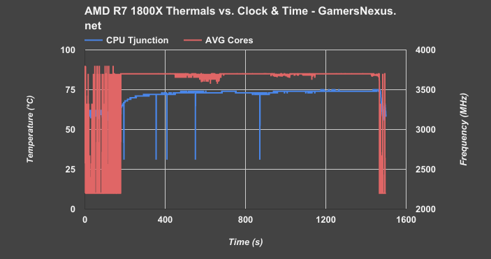
Above: Large Fourier Transform crunch
This first chart shows two things, primarily: We’re looking at CPU junction temperature in blue and averaged core frequency in red during a Prime workload. Ideally, the red line is perfectly flat when under heavy load, indicating a more stable core clock. The blue line should never exceed 75C, as that is AMD’s maximum junction temperature for the 1800X – or TjMax. We were able to trip a thermal shutdown by intentionally heating the CPU beyond 75C, validating that TjMax is in fact around 75C (+/-2C reading in AI Suite). Note that although the junction sensor is perfectly precise, it is not necessarily perfectly accurate – nor is software’s ability to interpret the sensor data. There may be latencies in some software solutions, and other differences in sensor accuracy could mean that you see temperature reports exceeding 75C; that does not mean Tjunction is actually >75C in reality, it just means that the sensor thinks that’s the case. Depending on what type of sensor is used, there are often accuracy ranges of 1-2.2C. Precision remains unimpacted by this. Using software which does not make adjustments to the raw junction output by the CPU means, like in the case of early AIDA64 revisions during this testing, that you may see temperatures ~20-30C below what reliable tools report.
We did our best with a combination of AI Suite and HW Monitor. Ryzen Master was not made available to media until we were on planes for an event. Prior to our finalized test run, we mounted thermocouples to the IHS to get an understanding of external case temperature, then compared that to a few other DUTs to build a knowledgebase of the temperature logging behavior on Ryzen. This was plotted versus various software solutions. We then removed those thermocouples and began temperature testing with our chosen two.
Gauging thermal performance on AMD isn’t exactly easy, and the diode reporting has some inconsistencies at times that manifest in the form of massive reported temperature drops.
Above: Cropped scale, same chart
If we zoom into the chart, you’ll see that the clock-rate (using an nT workload) becomes less stable and starts to fluctuate in increments of 25-75MHz once temperature approaches 73-75C. This is AMD’s internal sensors working with the clock to keep thermals under control, down-clocking in rapid intervals to keep thermals below 75C. In other words, “expected behavior.” This is a worst-case Prime workload with an NZXT Kraken X62 at maximum fan and pump speeds (X62 review here). We see these temperatures in endurance production workloads as well, e.g. 100% load with Blender. Anyone putting this chip under 100% load for long uptimes, like CPU rendering, should seriously consider a better cooler than the Noctua unit that is most commonly paired with the CPU.
Voltage, Clock, & Power vs. Application
We also logged voltages versus applications, clock, and power draw. Here’s a look at those sort of ad-hoc results:
| Auto vCore, 2933MHz RAM | Blender (nT) | Cinebench (1T) | POV-Ray (1T) | Idle |
| Total System Draw (Watts) | 185 | 92 | 94 | 60 |
| Core Frequency (GHz) | 3.7 | 3.7 - 4.1 | 4.1 | |
| Core Voltage (v) | 1.221 - 1.243 | 1.395 - 1.461 | 1.417 |
With 185W total system power consumption – again, this is for the full system – we see the Ryzen R7 1800X operating at a steady boost frequency of 3.7GHz when all cores are engaged. This number can boost to 4.1GHz when only two cores are engaged, leaving the rest at lower clocks during unutilized periods. The voltage to sustain Blender at this clock and 100% load ranges from 1.221 vCore to 1.243 vCore. Cinebench 1T pushes us up to 4.1GHz at times, but fluctuates between 3.7 and 4.1. This workload generates a voltage of about 1.395 to 1.461 vCore, with total system power consumption at 92W. Finally, POVRay 1T runs a 94W system power draw, with 4.1GHz fixed for the frequency – fully in XFR range – and a core voltage of about 1.417v.
Continue to Page 5 for the synthetic benchmarks.
3DMark TimeSpy Benchmark – AMD R7 1800X vs. i7-6900K, 7700K, more
Exiting the power, thermal, and voltage heuristics, we now look to our first tests. This initial lineup includes synthetics and validation of AMD’s claims regarding Cinebench. Once we’ve established a baseline with FireStrike, TimeSpy, and Cinebench, we can move to production workload encoding and to game benchmarking.
This first test is 3DMark’s TimeSpy benchmark, offering a Dx12 performance look in a synthetic environment. TimeSpy provides framerate numbers alongside its CPU scoring and total score. The numbers we care most about are the “CPU Score” and “CPU FPS” metrics, with “Total Score” serving more as a validation point.
Sorting by CPU score, the AMD R7 1800X comes out looking strong in our first synthetic benchmark. It’s not quite up to the i7-6900K’s performance in this test (stock – we do not downclock the Intel CPUs like AMD has done in its demo), but at $500, the proximity grants bragging rights to Ryzen. The R7 1800X performs within a couple percentage points (~4%) of the i7-6900K when both are stock. Overclocking Ryzen gets us nearly equal to the i7-6900K, but applying an OC to Intel’s $1000 K-SKU part pushes it far above the rest of the bench. Intel overclocks higher right now, and additional memory overclocking headroom can help in other memory-specific tasks.
Here’s the FPS chart:
These comprise the above scores (some runs may be averaged over multiple passes). Should provide a more relatable set of metrics, though we have actual games for that later.
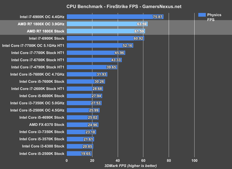
3DMark FireStrike Benchmark – AMD R7 1800X vs. i7-6900K, 7700K, 7600K
Moving on to 3DMark’s FireStrike suite at 1080p:
We’re sorted by physics score again.
In this benchmark, AMD looks pretty good. The R7 1800X falls prone only when we overclock the Intel i7-6900K to 4.4GHz, even when we also OC the 1800X to 3.9GHz (its maximum stable overclock on our bench). Still, landing where it does is, again, a feat worthy of note. We still have to look at real-world tests, but Ryzen starts off strong in synthetics, Cinebench (as AMD demonstrated), and some production workloads. The 1800X is at least marginally ahead of the i7-6900K when both are stock (19191 physics vs. 19401 physics, or a measured difference 0.67FPS – within FireStrike’s usual pass-to-pass variance).
Cinebench – AMD Ryzen R7 1800X vs. i7-6900K & Overclocking
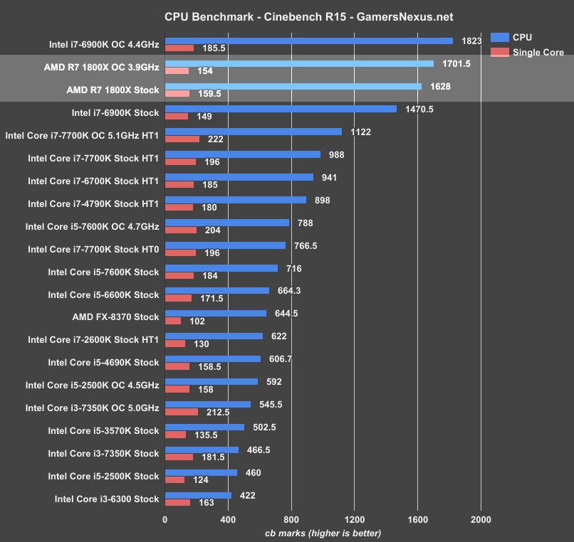
Cinebench isn’t everything, but early marketing slides might have you believing it is.
With Cinebench testing, the R7 1800X continues its synthetic lead from FireStrike. AMD is weaker when overclocked, but manages to best the 6900K (both stock) by roughly 10%. Note that 1T performance falls in the OC test as a result of XFR falling into disuse when manually tuning clocks, and so we actually reduced our 1T performance from 4.0-4.1GHz (variable) to 3.9GHz (forced OC). This is still better for nT performance.
POVRay Benchmark – AMD R7 1800X Overclocked, i7-6900K, 7700K
The Persistence of Vision ray tracer software (version 3.7.1 beta) offers a heavy CPU render test, where we use a standardized benchmark (not comparable with 3.6.x) for ray trace testing. POV-Ray can render atmospheric and particle effects, reflections, radiosity, and multiple light sources and bounces. We use the built-in single- and multi-threaded benchmarks (1T and nT, respectively).
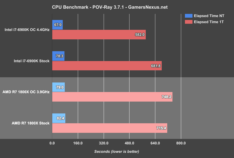
Intel pulls ahead in POV-Ray for both multi-threaded and single-threaded performance (again: 1T time increases on the OC 1800X as a result of the loss of XFR). We’re looking at 78.3s nT on the 6900K stock, or 82.4s on the 1800X stock. This test is conducted a minimum of three times and averaged.
Single-threaded, POV-Ray shows Intel holding a lead of about 33.6s (~4.7% reduction in render time.
We’ll move on to real-world rendering benchmarks for the next set of tests, using Premiere and Blender to provide that data.
Continue to Page 6 for the rendering benchmarks.
AMD R7 1800X Blender Benchmarks vs. i7-6900K, 7700K, 7600K, FX-8370
GN’s Andrew Coleman has several years of experience as a 3D animator, and so we are uniquely positioned to build our own rendering benchmarks and optimize render settings for the test. Blender does not work in its optimal state with out-of-box settings, and requires tuning tile size and compression settings for peak performance. CPUs, for instance, perform significantly better with smaller tile sizes (16x16), whereas GPUs tend to perform better in the 256x256 range, or thereabouts.
GN uses a custom-built Blender benchmark for its CPU rendering performance analysis. Here is a sample:

The benchmark mixes fur rendering (computationally intensive, particularly on GPUs), motion blur, ray tracing, multi-bounce light tracing, and various transparencies and mats.
In AMD’s marketing materials, the company used Blender for some of its initial tech day demonstrations that promised Intel’s 6900K – under some specific conditions – performing equally to AMD’s then-unnamed Ryzen CPU. AMD’s demonstration Blender benchmarks used different settings than what we would recommend. They were still deltas, so all is well in the world of comparisons, but it’s not an optimal test configuration for real Blender users. In its Blender testing, AMD executes renders using just 150 samples per pixel (what we consider to be “preview” quality), runs slightly unoptimized 32x32 tile sizes, and renders out at 800x800. In our benchmark, we render using 400 samples per pixel (release candidate quality), 16x16 tiles (faster for CPU rendering), and a 4K resolution. This means that our benchmarks are not comparable to AMD’s, but they are comparable against all the other CPUs we’ve tested. We also believe firmly that our benchmarks are a better representation of the real world.
Our Blender benchmark chart is below, and uses properly optimized benchmark settings (tile size, sample size, compression) for the test:
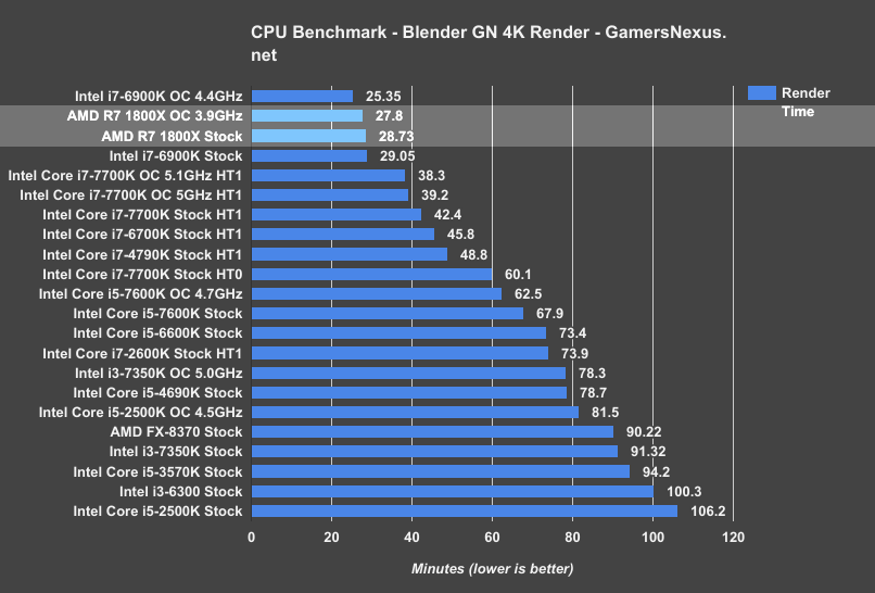
The AMD Ryzen R7 1800X completes the frame render in just under 28.73 minutes, with the Intel i7-6900K completing the render in 29.05 minutes. This puts AMD’s $500 Ryzen R7 1800X about on-par with the $1000 Intel i7-6900K for our Blender render task when both are in stock configuration. The R7 1800X is about 1-1.1% faster. Normally, this would be unsurprising or uninteresting, but the price makes AMD’s R7 platform worthy of further consideration.
Overclocked, we see the i7-6900K (~4.4GHz) reduce its render time to 25.35 minutes, while the Ryzen chip sits at 27.8 minutes. When overclocking is considered, AMD falls behind – but it’s still half the price, so consider both aspects.
As for other devices, the $340 i7-7700K (stock, HT1) completes the same render in 42.4 minutes, with the overclocked variant finishing in 38.3 minutes. We’re curious to see how the Ryzen R7 1700 holds up to the 7700K in this task.
For reference, the FX-8370 completes the render in 90.22 minutes, a far cry from today’s performance.
Blender is one of the few applications we tested where Ryzen shows its advantaged price-to-performance position, achieving mostly equal – slightly ahead, in some cases – render times to the $1000 6900K. This is because Blender is fully multithreaded, and tasks all threads to operate at full tilt until the render is done. Each tile of the scene is rendered by a single thread, and with 16 threads in flight, we see overall processing time reduce in a greater way than just increasing the frequency would do. This is demonstrated by looking between the 6900K and 7700K at 5.1GHz.
Of course, pushing it all to a GPU is normally much faster – a few times faster, in fact – making it tough to argue precisely when software accelerated rendering makes sense in Blender. Some specific elements of scenes will crunch better on a CPU, like heavy motion blur or (in previous versions of Blender) dense fur and hair. There’s potentially a valid use case in rendering from both ends of the animation and meeting in the middle, so to speak; that is, you might have the GPU render frame 1-1500, then have the CPU render from 1501-3000 (simultaneously).
Regardless, Ryzen holds a lead here, even if it does come down to a difference of 1.1% in an application that is normally (but not always) better GPU accelerated.
AMD R7 1800X Adobe Premiere Benchmark vs. i7-6900K, i7-7700K
Our video production workload is also a real-world test, pulling from files and export settings that we use every day for GN’s YouTube channel. The test is a render of our EVGA ICX review and includes dozens of audio, video, and image files loaded into it. Color correction, transforms, and other calculations (like Warp Stabilization) are included in the render, meaning that it is a precise representation of what we’d use Adobe Premiere CC for on a daily basis. This also means that the workload is computationally intensive, as the render is doing more than just encoding.
Our encoder settings are configured to 28Mbps target/max bitrate, with a “High” 5.1 profile. We are rendering at 1920x1080 and 60.0FPS (h.264).
Note: We only just added Adobe Premiere, so we’ve only got the three CPUs on the bench as of this review.
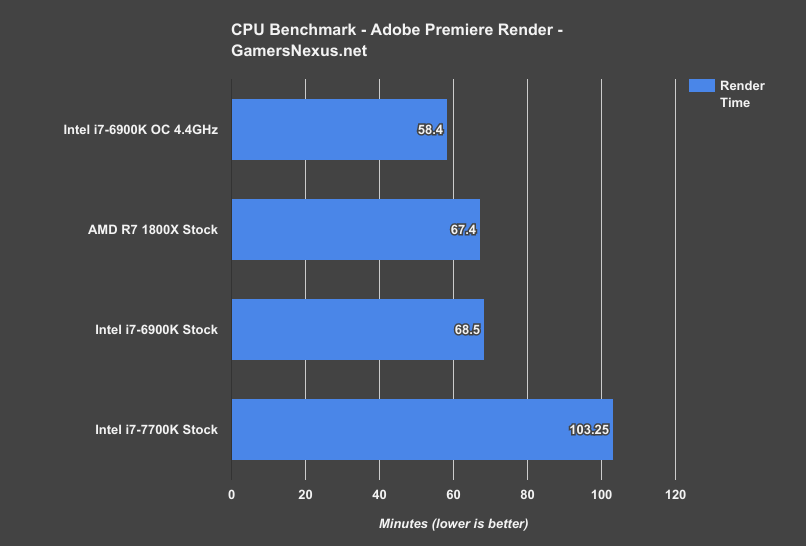
Configured to its stock clocks, the AMD R7 1800X completes the render task in 67.4 minutes, with the 6900K completing the video render in 68.5 minutes. If you prefer percentages, that’s a change of 1-2%. In rendering terms, you’d be saving about one minute for every hour of encoding. Ignoring all context, that’s not impressive, but context is what matters.
The context of Ryzen and the R7 1800X is that it’s a $500 CPU, and that high-end motherboards can be had for $255. Intel’s i7-6900K is $1000, and high-end motherboards cost $300 plus. Quad-channel memory is lost, but it’s also not all that beneficial in this specific test. The i7-7700K drags behind, completing the render nearly 40 minutes later than the 6900K and 1800X CPUs.
For Perspective: Adobe Premiere CUDA vs. CPU Benchmarks
That said, anyone running production renders knows that it’s the GPU that counts for most rendering tasks, despite some specific use cases where a high-end CPU can be beneficial.
For Premiere, we’d never use the CPU as the primary render workhorse. CUDA and OpenCL acceleration are significantly faster in supported applications.
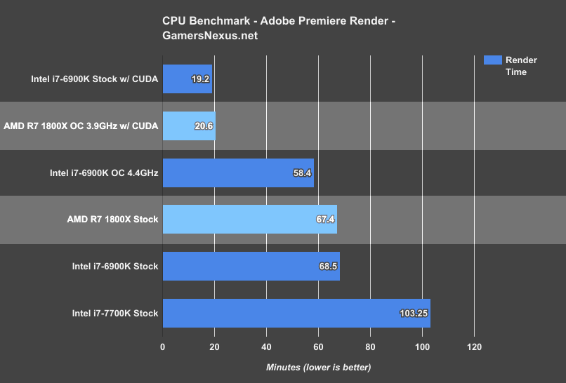
This chart puts our render numbers into perspective, relying instead on the EVGA GTX 1080 FTW and CUDA for the render.
The result is expected: Our render times drop from around 60 minutes to 20 minutes. Rendering on the CPU takes 3x as long, and using a Ryzen CPU + GPU is not any faster than using a 6900K + GPU to render, as the heaviest work is still going to the GPU. Even aa GTX 1070 would be significantly faster.
AMD does deserve praise for accomplishing comparable render speeds to Intel’s high-end CPUs, but we must also frame that praise within the confines of reality: For the type of production rendering most people do, using a high-end GPU makes infinitely more sense than software rendering. That’s not to say that there aren’t use cases for CPU-based rendering, it’s just going to be on users in those situations to determine their needs.
Continue to Page 7 for gaming benchmarks.
Note: If you've skipped every other page and come straight here, please consider reading the previous pages before posting comments with questions. The methodology page likely answers most basic questions.
Watch Dogs 2 Benchmark – R7 1800X vs. 7700K, 7600K, FX-8370
Our standalone Watch Dogs 2 CPU benchmark demonstrated the game’s propensity for multithreaded scaling, including utilization up to 16 threads on the 6900K (and now R7 1800X). WD2 stands as one of the best real-world gaming benchmarks for multithreaded CPUs, thanks entirely to its responsiveness to threads and (to a lesser extent) CPU frequency.
For additional research on Watch Dogs 2, check out our WD2 CPU Optimization guide, which talks graphics settings and the individual impact on CPU performance.
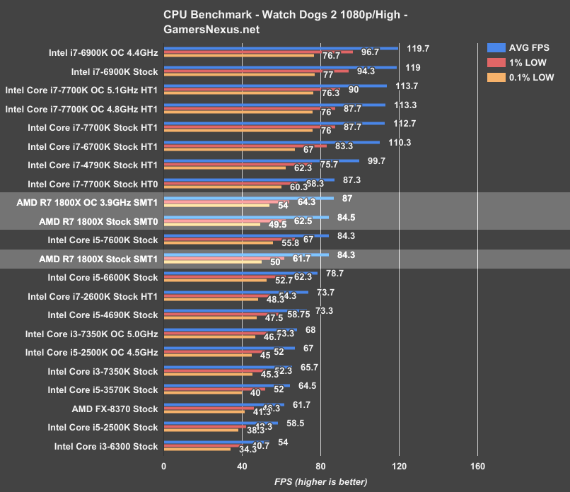
At 1080p/high (1440p test later on), we’re seeing the Intel i7-6900K (~$1000) top the charts at around 119FPS on the GTX 1080 FTW. The low percentile performance sits at ~94FPS 1% lows and 77FPS 0.1% lows. Comparatively, AMD’s R7 1800X (~$500) – the intended direct competitor to Intel’s i7-6900K – is operating at around 84FPS AVG, with 1% lows hanging around 62FPS and 50FPS (0.1%). In terms of raw FPS, that’s a performance delta of approximately 35FPS in averages (roughly 40%).
Comparatively, the Intel i7-7700K ($340) stock CPU (hyperthreading enabled) operates at around 113FPS AVG (1%/0.1%: 88FPS, 76FPS), with the i7-6700K Skylake CPU around 110FPS AVG. Even the Devil’s Canyon i7-4790K circa 2Q14 is outperforming the R7 1800X, placing at ~100FPS AVG.
Disabling hyperthreading on the i7-7700K plants us about equal with AMD’s R7 1800X (SMT enabled, so 8C/16T), further demonstrating an Intel architectural advantage outside of raw core/thread count; at least, an advantage in gaming workloads – AMD has already demonstrated a clear advantage in production workloads, shown on page 6 of this review.
Overclocking the R7 1800X pushes to 87FPS AVG, with marginal (read: unnoticeable) improvements in lows to 64.3 1% and 54 0.1%. The maximum sustainable overclock with our chip and motherboard seems to be about 3.9GHz, resulting in a percent increase of ~3.2% from stock (3.7GHz on all cores) to the overclocked variant.
Ultimately, for Watch Dogs 2, the 1800X performs mostly equally to an Intel i5-7600K ($240) CPU (previously reviewed here).
This illustrates quite clearly that just having more cores doesn’t win all arguments, but that’s something we’ve experienced time and again with CPU architectures. There’s more to architecture than just cores, threads, and clock speeds, as detailed on the first page of this review.
In fact, disabling SMT reveals that performance is largely the same in Watch Dogs 2 – though we’ll see a decrease in other games – netting an output of ~85FPS AVG versus the original 84.3FPS AVG. SMT doesn’t help AMD here, but let’s check Battlefield for a better idea.
Battlefield 1 Benchmark (Dx11) – R7 1800X vs. 6900K, 7700K, 2600K
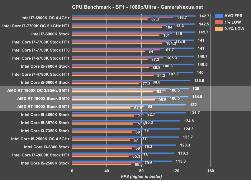
Moving on to Battlefield 1 (1080p/Ultra, Dx11), the i7-6900K and i7-7700K (overclocked – some loss in lows) are bumping against a wall around 140~142FPS, but we’re still seeing the high IPC and clock-rates of the i7-7700K ($340) planting the chip about equal to an i7-6900K. This remains true for the 6700K, i5-7600K, and i7-4790K. The i5-6600K begins to drag behind a little bit, at 137FPS AVG, and that CPU is trailed eventually by the AMD R7 1800X overclocked to 3.9GHz, landing at 135FPS AVG. The 1% lows hover around 108.5FPS, with 0.1% around 94FPS – considering the low percentile performance of neighboring chips, that’s good performance overall. Considering the price and age of nearby chips, the 1800X doesn’t look great in this particular benchmark. We do have a 1440p visit lower down, for what it’s worth.
Ultimately, the $500 AMD R7 1800X is effectively equivalent to an i5-4690K, which once retailed for $240. Tradeoffs abound, as usual, but one thing is clear: The 1800X is not impressive in the BF1 department, and is matched evenly by 2014 Intel architectures.
Disabling SMT on the R7 1800X results in performance that boosts to 134.5FPS AVG, up from 132FPS AVG. Because GamersNexus also measures frametimes, we benefit from the knowledge that disabling SMT further increases 1% low and 0.1% low metrics by upwards of ~30FPS (around 30% better 1% low values with SMT off).
Let’s move on for now, then loop-back later to see how imposing more of a GPU bottleneck impacts things.
Ashes of the Singularity (Dx12) – R7 1800X vs. 6900K, 7700K, 4790K
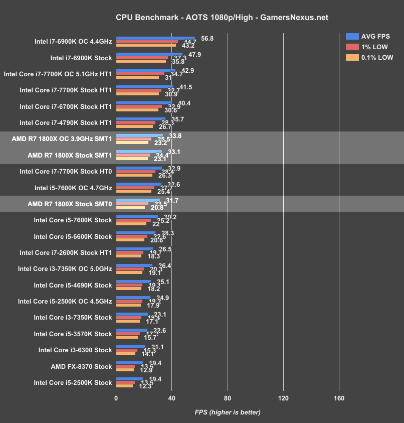
Ashes of the Singularity offers a glimpse into DirectX 12 performance, where we use the CPU-specific test and 1080p/High settings to pit processors against one another in a high-stress gaming workload. The i7-6900K at 4.4GHz plants us around 56.8FPS AVG, with low performance around 44.7 and 43.2FPS (1%, 0.1% respectively). This overclock is a significant gain over the 47.9FPS AVG of the 6900K stock, netting a jump of approximately ~15%.
For a more reasonably priced purchase for gamers, we look to the i7-7700K: Stock, the Kaby Lake CPU operates at 41.5FPS AVG with lows in the lower 30s. Overclocking to 5.1GHz pushes us to 42.9FPS AVG – not that impressive. The 1800X lands between the 7700K and 6900K in price, and falls below both in Ashes performance. AMD’s Ryzen R7 1800X CPU performs about where the 4790K performs, and just ahead of the i7-7700K with hyperthreading disabled. The R7 1800X outputs 33.1FPS AVG, with 1% and 0.1% lows in the 20s. Overclocking gains us marginal improvements at best, but that’s to be expected when limited to a 200MHz clock increase.
In the very least, this is a more defensible position than the 1800X’s outflanked standing on the Battlefield 1 chart – we’re no longer in territory of i5 CPUs from five years ago. We see again that cores and threads aren’t everything, given the lower-level intricacies of what exactly constitutes those cores.
Disabling SMT in Ashes of the Singularity results in a performance decrease of roughly 1-2FPS AVG, and so is insignificant overall. This game seems to get some slight benefit out of SMT.
GTA V – R7 1800X Benchmark vs. 6900K, 7700K, 2600K
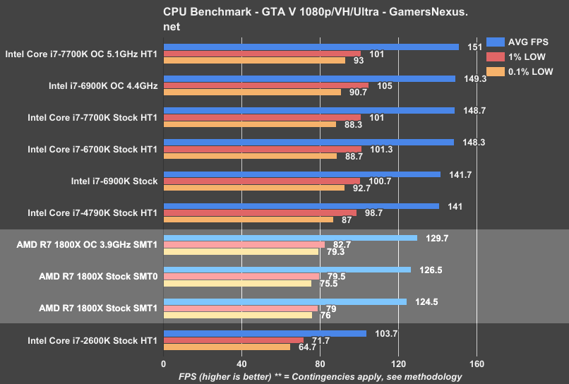
GTA has several issues in testing, but it’s not a problem if you know what they are. We eliminate four-core CPUs from this benchmark for methodological reasons. View here. Note that the game engine limits framerate to a hard ~187 (187.5, it seems), and so any CPUs performing in excess of this during spikes will not count the framerate with the greatest accuracy, as we run out of headroom. This means that the 6900K and 7700K OC CPUs are actually capable of higher averages, but the spikes exceed the engine framerate cap. We are working toward deprecating GTA V in our benchmark, but it still has usefulness for eight-core CPUs.
For GTA V, the AMD R7 1800X Stock (SMT0) operates at around 127FPS AVG, leading the 1800X Stock (SMT1) at ~125FPS AVG. This is repeatable and is not within “margin of error.” This performance puts the 1800X Stock (SMT1) about 20.1% faster than the 2600K, or about 13.3% slower than the i7-4790K from Devil’s Canyon. Compared to the i7-7700K (stock, HT1 vs. stock, SMT1), we see the 1800X is about 19.4% slower than the i7-7700K.
Overclocked, AMD pulls up to ~130FPS AVG (with an appropriate increase in lows). Compared to the OC’d 7700K at 5.1GHz, which is bumping hard against the framerate cap in some scenes, we see the 1800X decreases the theoretical maximum throughput by >16%.
Metro: Last Light - R7 1800X vs. 2600K, 7700K, 6900K
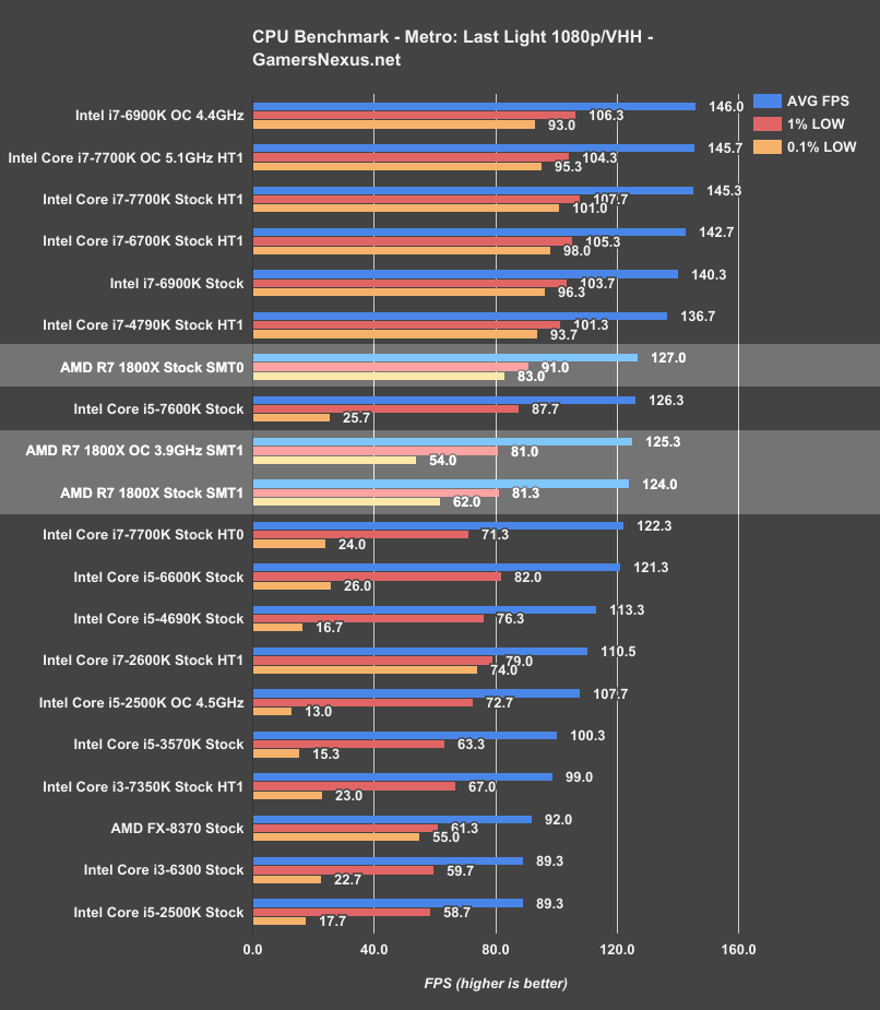
Metro: Last Light has historically penalized games in the 0.1% low department for two things: Threading and clock-rate stability. Overclocks that border instability are more likely to show poor 0.1% low performance, as are Intel i5 and i3 CPUs that operate on just four total threads. This is shown clearly in the 6600K and 4690K performance, where we have some bouncing around between low-end frametime performance (tends to become less repeatable, too; the ‘tightness’ of results decreases).
The AMD R7 1800X with SMT off performs the best of the AMD units, at 127FPS AVG and with lows at 91FPS (1%) and 83FPS (0.1%). This is behind the Intel i7-4790K (137FPS AVAG, 101/94FPS lows). Increased clock-rate of Intel CPUs also helps the company with its 7700K and 6900K chips, as MLL tends to favor >4 threads for frametimes, then clock-rate for overall throughput.
The AMD R7 1800X with SMT enabled (stock) operates at 124FPS AVG, or about 3FPS behind when SMT is disabled. Frametime performance also decreases with SMT, dropping from 83FPS 0.1% low to ~62FPS. We believe this is related to some sort of resource contention, though we are presently unclear on whether that’s more on the game side or the uCode/CPU side. AMD's cores do show a real advantage in Metro, and it's in the low frametime metrics. It's still not competing head-to-head with a cheaper i7-7700K, but the lows are better than i5s of comparable averages.
Total War: Warhammer (Dx11) – R7 1800X vs. 6900K, 7700K, 6700K
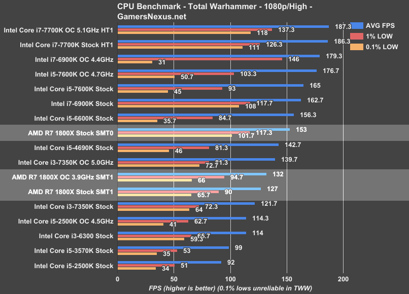
We’re still adding to our Total War: Warhammer benchmark listing. The game was only just added to our charts in time for the i5-7600K review & i5-2500K revisit articles, and so i7 CPUs haven’t been fully subsumed by the Warhammer bench. Thus far, we’ve added the i7-7700K and i7-6900K, alongside all the usual i5/i3 suspects (and the FX-8370). Warhammer is also finnicky about overclocking stability, as you’ll see with the low frametime metrics in the 6900K OC values.
Total War is one of the most CPU-intensive game series we’ve worked with, right up there alongside Watch Dogs 2. That said, the game does appreciate clock-speed to a great extent: we see the tradeoff between cores and frequency when ricocheting between the i7-7700K and i7-6900K processors. The i7-7700K pulls ahead in every regard when pitted against the 6900K, thanks to its 4.5GHz and 5.1GHz clocks, and lands around 186~187FPS AVG. Our lows (stock) operate at 126FPS 1% and 111FPS 0.1%; overclocking pushes those to 137FPS 1% and 118FPS 0.1% low.
As for the Ryzen R7 1800X, the new Zen arch CPU lands between the i3-7350K ($180) stock and 5.0GHz overclocked variant (reviewed here). Total War shows a clear frequency focus, further emboldened by the 1800X’s ~5FPS (~4%) FPS increase from a 200MHz overclock. Partly for this reason, among other architectural advantages, Intel again holds the lead even with processors of significantly lower cost. We still wouldn’t recommend that you go out and buy an i3-7350K (at least, not at $180), but the 1800X performs just slightly better than the overpriced (but still cheaper) i3 K-SKU.
Total Warhammer shows the biggest change in performance when disabling SMT. The AMD R7 1800X moves from ~127FPS AVG (1% low: 90, 0.1% low: 65.7) to ~153FPS AVG with SMT0. That’s an increase in performance of 20.5% by disabling AMD’s most advertised property. In the 1% and 0.1% low values, AMD moves from 90 to 117.3FPS (1% low) and from 65.7 to 101.7FPS (0.1% low), indicating further that SMT hamstrings frame latency significantly.
1440p Benchmarks (Introducing a GPU Bottleneck)
When we approached AMD with these results pre-publication, the company defended its product by suggesting that intentionally creating a GPU bottleneck (read: no longer benchmarking the CPU’s performance) would serve as a great equalizer. AMD asked that we consider 4K benchmarks to more heavily load the GPU, thus reducing workload on the CPU and leveling the playing field. While we fundamentally disagree with this approach to testing, we decided to entertain a mid-step: 1440p, just out of respect for additional numbers driven by potentially realistic use cases. Of course, in some regard, benchmarking CPUs at 4K would be analogous to benchmarking GPUs at 720p: The conclusion would be that every GPU is “the same,” since they’d all choke on the CPU. Same idea here, just the inverse.
We’ve only run a few CPUs for these tests, since they’re not part of our standard bench. Here’s a look at Watch Dogs 2 at 1440p/High:
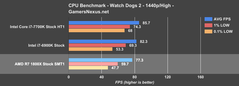
The AMD R7 1800X – even when taking AMD’s suggestion of burdening the GPU (again, we don’t necessarily agree with this methodology) – is still performing at a framerate deficit to the cheaper i7-7700K. Now, of course, the next argument might be that the visible difference between 86FPS and 77FPS AVG is not profound – and that’d be a fine argument. Unfortunately, it still doesn’t make sense to spend more money and get less. That’s just bad value; besides, when considering the CPU and platform tend to last the longest in a system, the upgrade pathways (to stronger GPUs) are going to be better on the platform which has the highest baseline performance.
The next argument might be that mixed workload users, like content creators, would benefit from the production advantages afforded by Ryzen. That’s a much stronger argument, but still has caveats and counters; we’ll point you back to Page 6 for that discussion.
All that said, let’s look back to the numbers one more time: Frametimes suffer a bit with the 1800X, falling to ~48FPS 0.1% low and ~60FPS 1% low versus the 7700K’s ~68FPS 0.1% low and ~74FPS 1% low metrics. This isn’t something where we’re seeing stuttering (you’d have to fall lower for that), but it does indicate that AMD has other potential weaknesses that could emerge under the right conditions.
Moving on to Battlefield 1 at 1440p, where we’re definitely developing a GPU bottleneck (and beginning to invalidate the wants of 120/144Hz users), we see similar hierarchy:
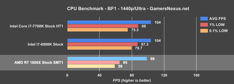
Ryzen’s R7 1800X, using the GPU as a crutch, is now more or less on-par with the 7700K and 6900K CPUs (demonstrably GPU bottlenecked). We’re still seeing decreased frame latency versus Intel, but like with Watch Dogs 2, that’s not producing any noticeable stuttering to the end user – it’s just a measurable difference.
In this particular title, benchmarking incorrectly does in fact make the numbers look better for AMD – but the 7700K still outperforms the 1800X, and the 7700K is still cheaper. We’ll have to see how the R7 1700 ($330) performs for a better glimpse at AMD’s future as a competitive performer in video games.
Continue to Page 8 for the conclusion.
AMD Ryzen R7 1800X Conclusion
At this point, you might be left feeling disillusioned when considering AMD’s tech demos. Keep in mind that most of the charts leaked and created by AMD revolved around Cinebench, which is not a gaming workload. When there were gaming workloads, AMD inflated their numbers by doing a few things:
In the Sniper Elite demo, AMD frequently looked at the skybox when reloading, and often kept more of the skybox in the frustum than on the side-by-side Intel processor. A skybox has no geometry, which is what loads a CPU with draw calls, and so it’ll inflate the framerate by nature of testing with chaotically conducted methodology. As for the Battlefield 1 benchmarks, AMD also conducted using chaotic methods wherein the AMD CPU would zoom / look at different intervals than the Intel CPU, making it effectively impossible to compare the two head-to-head.
And, most importantly, all of these demos were run at 4K resolution. That creates a GPU bottleneck, meaning we are no longer observing true CPU performance. The analog would be to benchmark all GPUs at 720p, then declare they are equal (by way of tester-created CPU bottlenecks). There’s an argument to be made that low-end performance doesn’t matter if you’re stuck on the GPU, but that’s a bad argument: You don’t buy a worse-performing product for more money, especially when GPU upgrades will eventually out those limitations as bottlenecks external to the CPU vanish.
As for Blender benchmarking, AMD’s demonstrated Blender benchmarks used different settings than what we would recommend. The values were deltas, so the presentation of data is sort of OK, but we prefer a more real-world render. In its Blender testing, AMD executes renders using just 150 samples per pixel, or what we consider to be “preview” quality (GN employs a 3D animator), and AMD runs slightly unoptimized 32x32 tile sizes, rendering out at 800x800. In our benchmark, we render using 400 samples per pixel for release candidate quality, 16x16 tiles, which is much faster for CPU rendering, and a 4K resolution. This means that our benchmarks are not comparable to AMD’s, but they are comparable against all the other CPUs we’ve tested. We also believe firmly that our benchmarks are a better representation of the real world. AMD still holds a lead in price-to-performance in our Blender benchmark, even when considering Intel’s significant overclocking capabilities (which do put the 6900K ahead, but don’t change its price).
As for Cinebench, AMD ran those tests with the 6900K platform using memory in dual-channel, rather than its full quad-channel capabilities. That’s not to say that the results would drastically change, but it’s also not representative of how anyone would use an X99 platform.
Regardless, Cinebench isn’t everything, and neither is core count. As software developers move to support more threads, if they ever do, perhaps AMD will pick up some steam – but the 1800X is not a good buy for gaming in today’s market, and is arguable in production workloads where the GPU is faster. Our Premiere benchmarks complete approximately 3x faster when pushed to a GPU, even when compared against the $1000 Intel 6900K. If you’re doing something truly software accelerated and cannot push to the GPU, then AMD is better at the price versus its Intel competition. AMD has done well with its 1800X strictly in this regard. You’ll just have to determine if you ever use software rendering, considering the workhorse that a modern GPU is when OpenCL/CUDA are present. If you know specific in stances where CPU acceleration is beneficial to your workflow or pipeline, consider the 1800X.
For gaming, it’s a hard pass. We absolutely do not recommend the 1800X for gaming-focused users or builds, given i5-level performance at two times the price. An R7 1700 might make more sense, and we’ll soon be testing that.
AMD defends its position by indicating the ISVs need to begin supporting their product, and has provided us statements from StarDock and Bethesda relating to this. To these statements, we’d remind folks that games take a long time to develop. Buying a CPU now in the hopes that games will better leverage 16T CPUs in a few years is a risky move – particularly with Bethesda’s track record for game optimization.
Regardless, we’ll provide the quotes that AMD passed along:
“Oxide games is incredibly excited with what we are seeing from the Ryzen CPU. Using our Nitrous game engine, we are working to scale our existing and future game title performance to take full advantage of Ryzen and its 8-core, 16-thread architecture, and the results thus far are impressive. These optimizations are not yet available for Ryzen benchmarking. However, expect updates soon to enhance the performance of games like Ashes of the Singularity on Ryzen CPUs, as well as our future game releases.” - Brad Wardell, CEO Stardock and Oxide
Note that the above was in response to poor performance of the 1800X in Ashes of the Singularity.
And:
"Creative Assembly is committed to reviewing and optimizing its games on the all-new Ryzen CPU. While current third-party testing doesn’t reflect this yet, our joint optimization program with AMD means that we are looking at options to deliver performance optimization updates in the future to provide better performance on Ryzen CPUs moving forward. " – Creative Assembly, Developers of the Multi-award Winning Total War Series
This, we believe, was a response to the Total War: Warhammer performance that we observed, given Creative Assembly’s previous partnerships with AMD to promote the FX-6350 CPUs.
AMD’s best wasn’t enough for gaming workloads. If production is your thing, check the relevant benchmark page for more information. The price:performance in that category is the one saving grace for the R7 1800X.
The R7 1700 may prove a better value for gaming; we’ll have those benchmarks shortly. For now, though, the 1800X is a disappointment, and is not a processor we recommend for gamers when considering the price-point. If you were to buy it, disable SMT for gaming. It’s mostly detrimental, likely due to resource contention among threads in gaming environments. Even mixed workload users should consider when and where software acceleration is better than GPU acceleration, if ever for their needs, before purchasing the 1800X. Do the research on your applications. For what we do with media production, it makes no sense to render software-accelerated; that doesn’t mean it never makes sense.
But yes: The 1800X is an impressive competitor to the 6900K in production, and it’s significantly cheaper. We’d recommend the 1800X over the 6900K for folks who genuinely use software acceleration. It’s just not good for gaming, and GPUs kill both AMD and Intel CPUs in accelerated rendering.
If you're on this page without reading the others, we'd suggest taking a second look back over them. The review is dense with information and took a significant effort to complete.
Update: 1700 review here.
Editor-in-Chief & Test Lead: Steve Burke
Sr. Editor & Tester: Patrick Lathan
Video Producer: Andrew Coleman
Additional Video: Keegan Gallick
To the team: Thank you for assisting in accomplishing this tremendous feat in just 4-5 days, while also sustaining travel across the country four times in the past week.