A significant aspect of any silicon engineering lifecycle is chip post-mortem, providing engineers with insight to a chip's inadequacies and specific points of failure; as the manufacturing process continues to decrease in physical size (we're nearing sub-20nm on most commercial microprocessors), increasingly powerful scopes are required to analyze internal electrical defects.
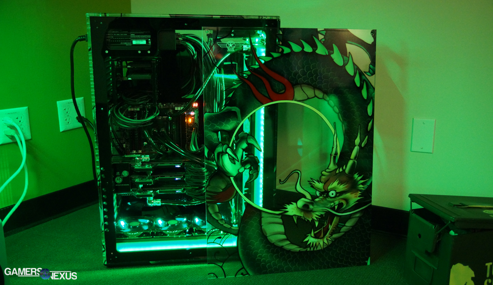 This is how nVidia does system building: A custom Danger Den box outfitted with custom sleeving and lighting.
NVidia Silicon Technology Failure Analysis Director Howard Marks gave us a walkthrough of some of the lab's multimillion-dollar analytical tools, seen in the video below. If this sort of content interests you, we'd also recommend checking out our recent walkthrough of Kingston's automated SMT lines and shipping robotics facilities.
What is Silicon Failure Analysis?
The Silicon FA department of any chip manufacturer/designer is responsible with studying the cause and specific point of failure on devices. That point could be an individual transistor, a trace, impedance caused by interfering components, or any number of other complex interactions. This information is then relayed to relevant engineering departments, which work to address the issue (ideally prior to launch) and resolve it.
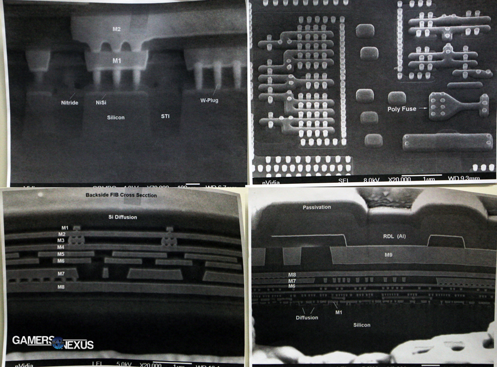 A sample of the images produced by the lab's equipment.
Because modern semiconductors use billions of transistors in the 20-30nm fab process range, powerful scopes and imaging machines are required to create magnified images for accurate analysis of the silicon. The image data is then fed into software that can further aid engineers in dissecting electromagnetic signal integrity issues or other potential agents for defects.
Due to time constraints, we limited our equipment showcase to the three machines demonstrated in the above video. In order, here's what you're looking at:
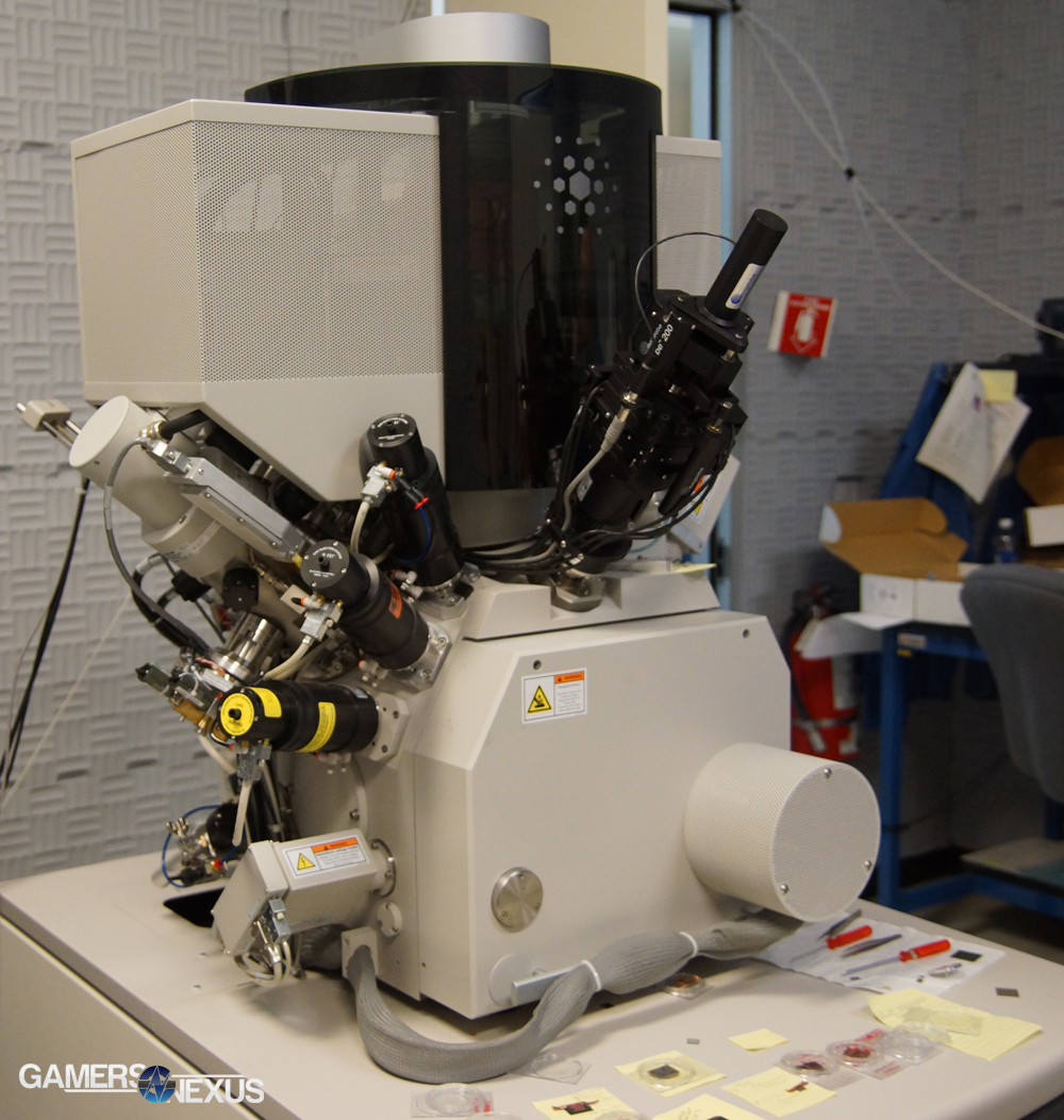 FEI's Helios NanoLab 600i focused-ion beam scope. FEI's Helios NanoLab 600i focused-ion beam scope. | 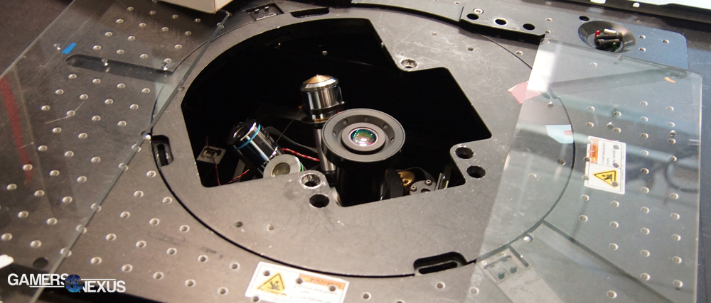 A Hubble Telescope-class camera used for photon emission probing on failing chips. A Hubble Telescope-class camera used for photon emission probing on failing chips. |
- A focused-ion beam machine by FEI (with a scanning-electron microscope that magnifies 1.5 million times and produces an image at a 7-angstrom resolution, or 7x10^-10 meters). The machine is used for cross-section analysis, wherein a heavy gallium ion is used to mill into the device under test (DUT) and expose the failing component's internals. Buying one of these for your foyer will set you back approximately $2.6mm.
- A 3D X-Ray. This monolithic piece of equipment takes thousands of scans from all angles of the DUT, providing 3D x-ray imaging of the chip, its substrate, the PCB, and all the transistors and numerous other surface-mount components. By creating a 3-dimensional x-ray image of the chip, nVidia's failure analysis team can see all aspects of the DUT from all angles, and can digitally dissect the image for study. Thousands of x-ray images are compiled into a seamless movie (shown in the above video). Marks told GN that "it used to take 11 hours to make that [photo-to-video] conversion, now - using a CUDA card - it takes only 3 minutes to make that same conversion."
- The final demonstrated analytical tool is nVidia's backside probing emission system, noteworthy for its use of camera equipment similar to what's found in the Hubble Space Telescope. Marks explained its function best, stating:
"When a transistor turns on inside a device, electrons travel through the semiconductor channel and give off photons; they give off both infrared photons in the thermal range and in the emission range. We can look and find out where the failing transistor is. This is an upside-down camera, so we can put a PC on top of here and actually look inside the chip while it's running an application. It [uses] the same kind of camera used in the Hubble Telescope, used to look at little points of light from the stars, which is the same infrared light that comes out of our chip when a transistor turns on. The camera is kept at liquid nitrogen temperatures in order for the camera not to contribute any heat to the source. We can see all the way down to the transistor and see how it behaves."
Of course, Howard Marks' lab wasn't the only noteworthy stop on our walk-through.
Other Aspects of our nVidia Tour
The Failure Analysis lab was easily the highlight of our tour through nVidia, but we hit a few other interesting demos along the way. Let's start with some photos:
 |  Click for hi-res. Click for hi-res. | 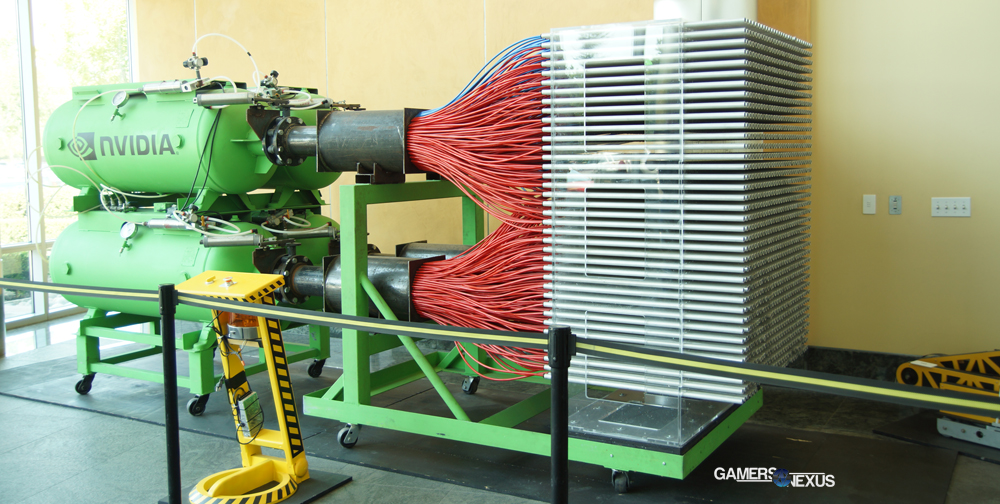 |
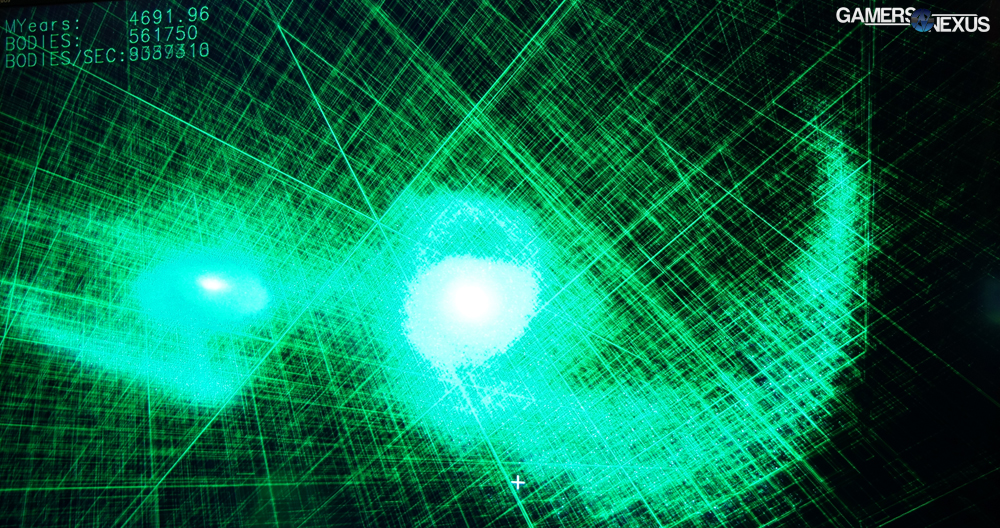
NVidia's demo room showcases graphics processing feats, like the above render/simulation of the Milky Way galaxy's impending collision with Andromeda; in this demonstration, more than 15,000,000 simultaneous objects are tracked and rendered to the screen using a Titan-powered render box. Each individual object (star) can be seen on a 6-axis grid and is tracked from pre-to-post collision.
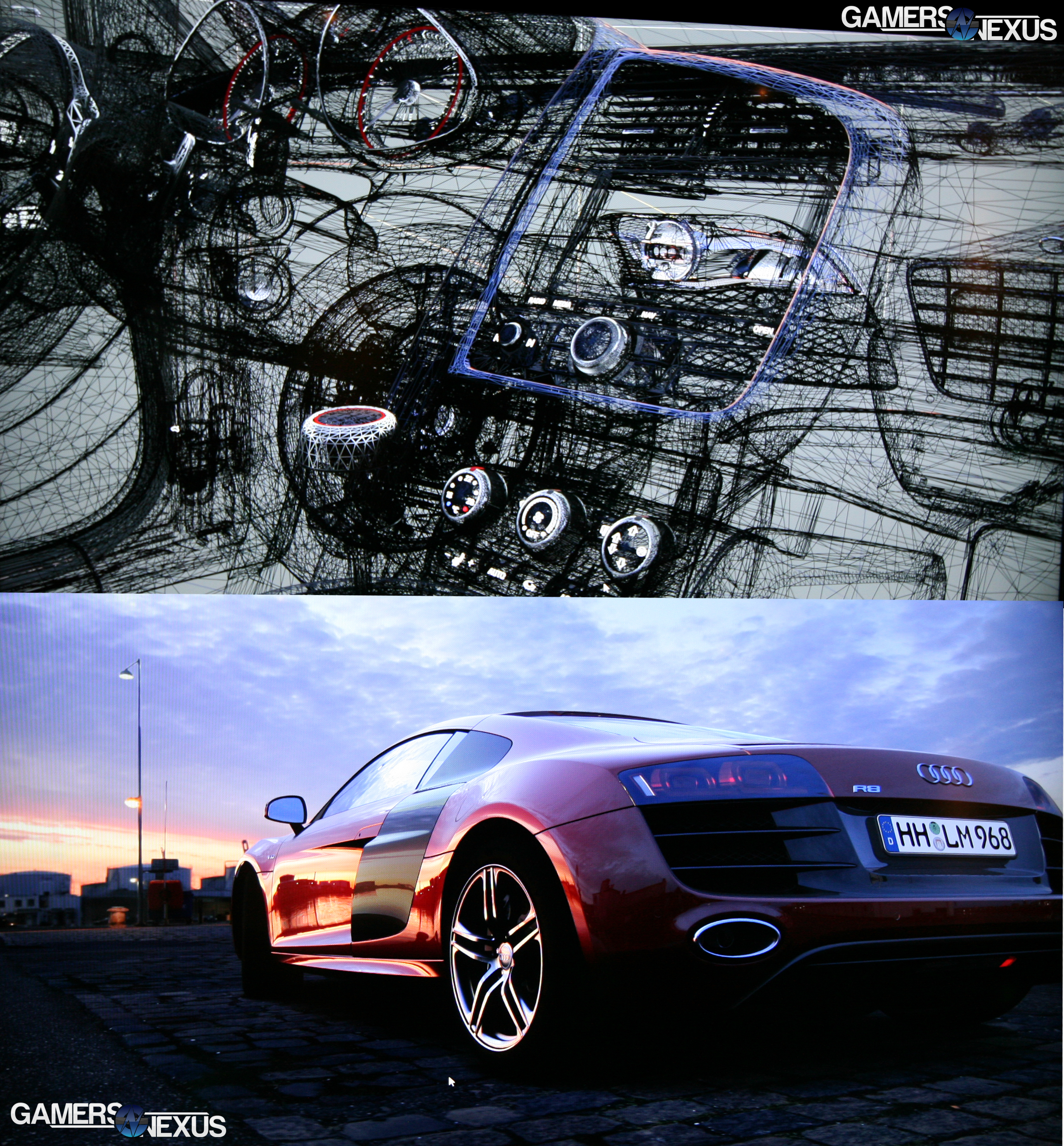
We were also shown real-time car renders done by Audi Motors, who use modeling software powered by professional-class nVidia GPUs to create immersive automotive samples. In the vehicle you're looking at above (figure 2), a total of 7 million polygons were used to create a true-to-life, full 3D model (interior & exterior) of the car prior to production. If you need that put into perspective, our interview with Star Citizen's Chris Roberts revealed that the average FPS character is comprised of between 10,000 and 30,000 polys.
 While browsing the nVidia campus, we also encountered the famed Mythbusters duo Adam & Jamie's parallel processing paint cannon. If you're not familiar with the video -- and you definitely should be -- Adam Savage and Jamie Hyneman constructed what is effectively a massive paintball machine gun, used to demonstrate parallel vs. sequential task execution. The cannon is an amalgamation of "thousands of pounds of aluminum and steel, a mile of high-pressure air hose, [and 1100 paintball barrels]," capable of firing 1100 individually-addressed bullets.
That about wraps up the more immediately interesting elements of our tour. Check back in the future for further nVidia content, including explanations of frame-time testing and the industry's shift in benchmarking analytics.
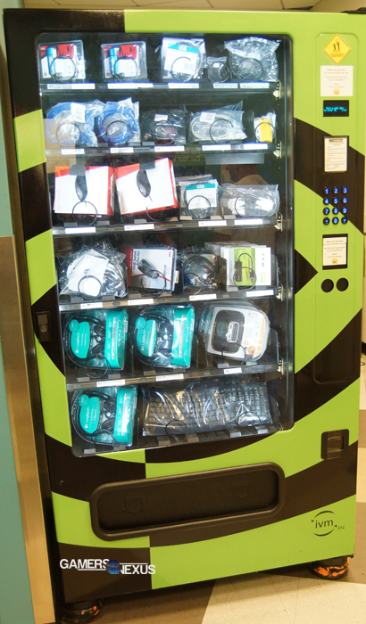
Oh, and because it's mildly amusing, here's a photo of a vending machine stocked with peripherals and electronics.
- Steve "Lelldorianx" Burke.