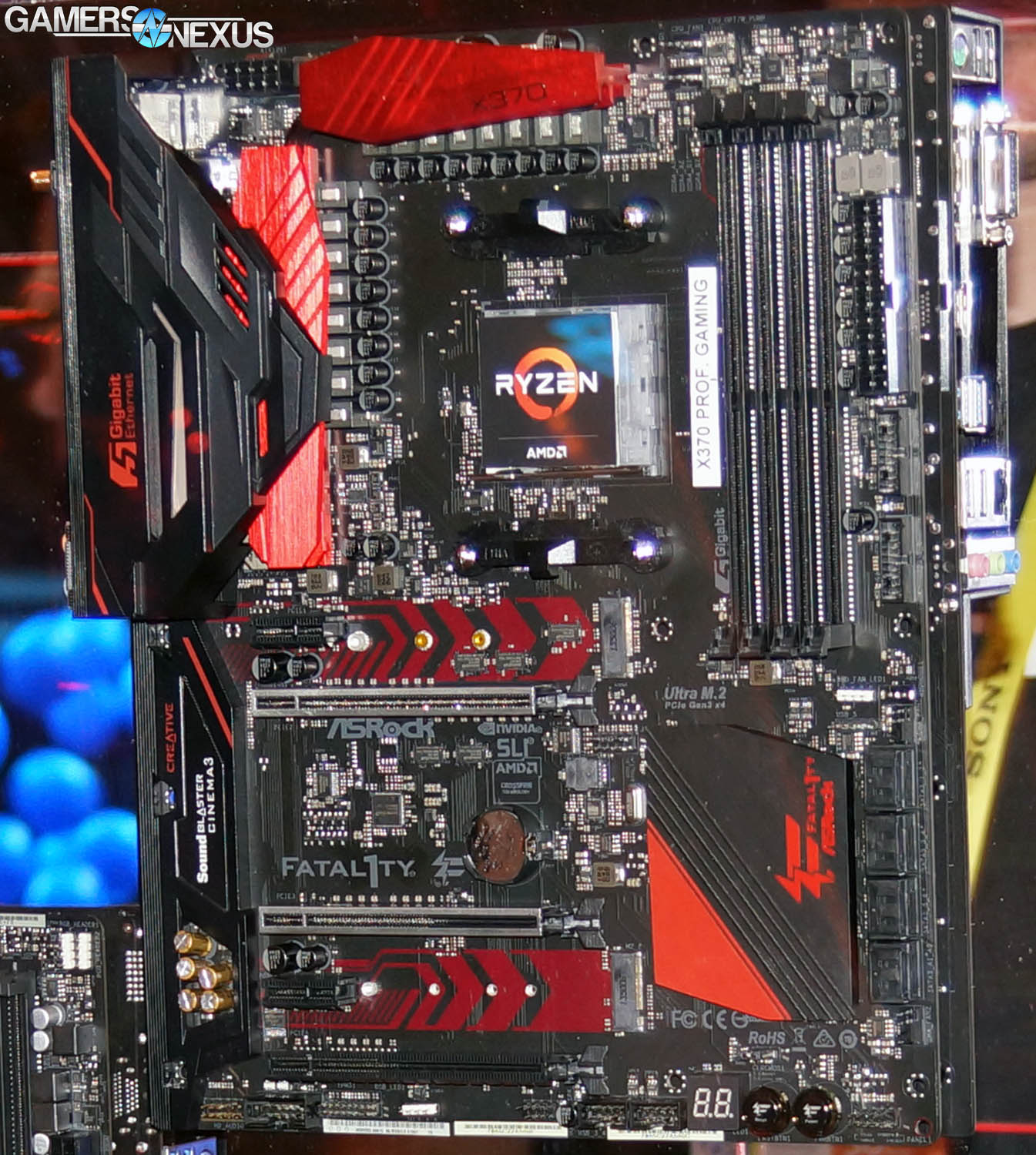
AMD’s Ryzen platform is on its march to the launch window – likely February of 2017 – and will be pushing non-stop information until its time of delivery. For today, we’re looking at the CPU and chipset architectures in greater depth, following-up on yesterday’s motherboard reveal.
First, let’s clear-up nomenclature confusion: “Zen” is still the AMD next generation CPU architecture name. “Ryzen” is the family of CPUs, comparable to Intel’s “Core” family in some loose ways. Each Ryzen CPU will exist on the Zen architecture, and each Ryzen CPU will have its own individual alphanumeric identifier (just like always).
That aside, we’ve created a block diagram (below) to detail the first line of Ryzen CPUs that have been revealed to us. This helps set the stage for explaining the differences between X370, B350, A320, and X300 AM4 chipsets.
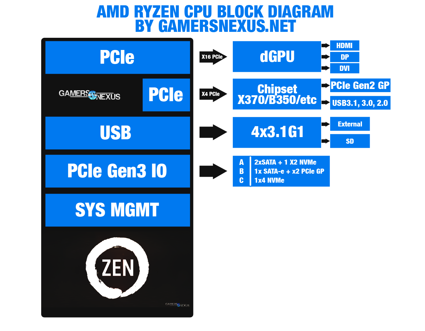
As printed in our motherboard article yesterday, most of the I/O is now handled on the CPUs themselves, making for more of an SOC approach rather than relying on a PCH or chipset for high-speed IO. This means that the CPU now carries all the relevant lanes for USB, SATA, NVMe, and PCIe general purpose use, with the chipset offering a few extra lanes and IO devices here and there.
X370, for instance, adds an additional 4x USB3.1 Gen1 options over B350, and both X370 & B350 have an extra 1x USB3.1 Gen2 option over the A320 chipset. PCIe Gen2 general purpose lanes are also incremented by 2 with each step (A320 starting at x4 PCIe Gen2). More significantly, the chipset also dictates overclocking and multi-GPU to some extent, with X370 explicitly permitting multi-GPU (split into x8/x8, or using muxers to achieve three GPUs). A320 does not allow overclocking where B350 and X370 do, though we’re not clear on if B350 and X370 may have different options in UEFI.
Regardless, the big thing to note here is that chipsets are far less significant than they used to be. You could get by just fine with B350 for the majority of mainstream cases, based strictly on the on-paper specs, and would only need X370 for multi-GPU setups or enthusiast-specific options that motherboard vendors will gate based on platform.
PCIe Gen3 lanes for graphics are all on the CPU, with the currently known 8C/16T Ryzen chip hosting 16 PCI-e 3.0 lanes for the GPU. These can be assigned to a single device or split in x8/x8 fashion (or multiplexed down to an x4 setup), but will be entirely reserved for the GPU. Other devices on the PCI-e bus, like M.2 devices, will draw from general purpose or chipset lanes. Four PCI-e Gen3 lanes are sent to the chipset to handle its I/O, and are then split amongst the connected devices.
You might have noticed that SATA Express is also on the block diagram, and may have even appropriately scoffed at the sight. Keep in mind that SATA Express, although largely a dead interface, is more valuable for its usefulness as an easily split set of lanes. SATA Express can become regular SATA III or can be pulled into M.2 duties.
The smaller chipsets are significantly different – X300 and A/B300 are all miniscule in physical area and serve almost entirely to function as a secure boot address. They offer no additional IO, leaving all input/output to transact through the CPU proper. The X300 chipset is targeted at mini-ITX motherboards and, as a side benefit, will provide some additional real-estate by its nature of taking less physical space. A/B300 chipsets will also fit this class, though are locked for overclocking where X300 is not.
For sake of clarity, here’s a table with all the IO differences between the chipsets:
Ryzen Chipset Differences
| X370 | B350 | A320 | X300 | A/B300 | |
| USB 2.0 | 6 | 6 | 6 | 0 | 0 |
| USB 3.1 G1 | 6 | 2 | 2 | 0 | 0 |
| USB 3.1 G2 | 2 | 2 | 1 | 0 | 0 |
| SATA | 4 | 2 | 2 | 0 | 0 |
| SATA Express (2x SATA III or 2x PCIe 3.0) | 2 | 2 | 2 | 0 | 0 |
| PCI-e 2.x | 8 | 6 | 4 | 0 | 0 |
| SATA RAID | 0, 1, 10 | 0, 1, 10 | 0, 1, 10 | 0, 1 | 0, 1 |
| Multi-GPU | Yes x8/x8 or multiplexed | No | No | Yes | No |
| Overclocking | Yes (Requires better cooling) | Yes | No | Yes | No |
SATA Express can split, again, into 2x SATA III, 2x PCI-e 3.x, or can merge with PCI-e GP lanes to create a 4-lane PCI-e port.
That’s all there is to these chipsets. Simple, this time around.
Editorial: Steve “Lelldorianx” Burke
Video: Andrew “ColossalCake” Coleman
Video: Keegan “HornetSting” Gallick