Intel’s latest memory technology has big aspirations. It has the ability to one day unify the DRAM and non-volatile memory structure, but we’re not there yet. Today, we get the Data Center Optane SSD (the DC P4800X) as a responsive, high-endurance drive specifically targeted at big data users. This is not a consumer product, but the architecture will not change in any significant ways as Optane & 3D Xpoint move to consumer devices. This information is applicable across the user space.
Upon initial release, the DC P4800X drive will be a 375GB PCIe 3.0 x4 NVMe HHHL device costing $1520 without Intel’s software, and $1951 with the Intel Memory Drive Technology software package. Later in the lifecycle, we should see 750GB and 1.5TB versions. The Optane SSD is one of three Optane technologies that Intel is marketing: Optane DIMM (fits into a DDR4 slot), Optane SSD (fits into a PCIe 3.0 x4 slot or U.2 connector), and Optane Memory (fits into an M.2 slot).
To clear a few things up straight away, Intel’s “Optane” is the company’s platform and related devices. Optane can function across standard interfaces (PCIe, U.2, DDR4, M.2) and does not require a new interface. 3D Xpoint is the underlying architecture, and is what Intel worked with Micron to produce. Each company contributed to 3D Xpoint, and each company has a spin-off platform built around the architecture. For Intel, that’s Optane; for Micron, it’s QuantX.
Intel Optane DC P4800X Specs
| Capacity | 375GB |
| Form Factor | AIC HHHL |
| Interface | PCI-e 3.0 x4 |
| Protocol | NVMe |
| Advertised Latency R/W | <10us |
| Advertised Throughput | 4K Random R/W IOPS: 550/500k 4K Random R/W 70/30: “Up to 500K” |
| Endurance | 30 drive writes per day (JESD219 workload) 12.3 PBW |
3D Xpoint and Optane will come to consumer at some point. It would not be unrealistic to expect a 1-year timeframe, given Intel’s cadence with server CPU technology bleeding into the consumer space. Everything we’re discussing today is applicable toward what consumers will eventually receive.
Intel Optane Implementation
The P4800X that becomes available today is meant for servers using Xeon processors and compatible motherboards, so you’ll need at least E5-x6xx v2 or E7-x8xx v2 or better. The drive can be used as a supplement to system memory or as storage. This choice is configurable upon boot through something like an Option ROM, which is powered by a new software called Intel Memory Drive Technology. The software, which has an added cost of ~$400, makes configuration simpler and provides optimizations that Intel claims are noticeable. A server administrator can use the software to choose from a pool of Optane SSDs and allocate them to either system memory or storage, but not both. When asked about adding the ability to segment a single Optane SSD as both memory and storage, Intel hinted that the feature may become available at a later date as dependent upon user demand.
There are limitations to the expansion of the technology. Most notably, system memory expansion is not recommended to exceed 8x the amount of DRAM installed, and each 375GB Optane SSD is only good for 320GiB of system memory expansion. It also appears that only the AIC is usable as system memory, not the U.2 version.
The Optane Solution
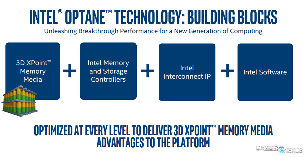
Looking more closely, the Optane solution is a combination of 3D Xpoint memory media, Intel memory and storage controllers, Intel interconnect IP, and Intel Software.
The 3D Xpoint memory media is a solid-state architecture that we previously defined here. The memory and storage controllers, we are told, work similarly to flash NAND SSD controllers with some notable exceptions. We’ll likely discuss these in detail when GN has a similar product for review and testing. The interconnect IP and Intel software portion appears to be a combination of licensed software from a company called ScaleMP and in-house developed code. ScaleMP is a company that specializes in virtualization and symmetric multiprocessing. Their technology allows a single piece of software to take advantage of a large number of aggregate CPUs and massive amounts of shared memory, an applicable match for making Optane work flexibly throughout the memory architecture.
The Controller
One of the controller’s most interesting jobs is adapting the 3D Xpoint memory media to the NVMe interface. The storage is architected at the byte level (making it usable as future DIMMs or as storage), but it must be adapted to block level so that it can communicate via NVMe’s recommended 4KB block schema. We’re not exactly sure how it’s doing this and, again, we hope to take a closer look at this once we get a sample in our bench. What we were told is that one 4KB transaction is spread across multiple channels and die using the proprietary programming of Intel’s controller.
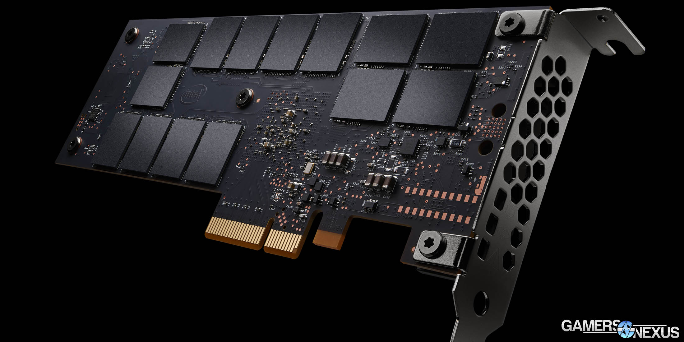
In the above image, we can clearly see 14 packages. It is likely that these Optane modules, like NAND Flash, are opposite the heat spreader because they may perform more optimally at higher temperatures. It is also highly likely that the controller is on the opposing side of the PCB, beneath the heatsink, to prevent thermal throttling under heavy data center workloads. One other related fact from Intel is that the initial 375GB P4800X has a total of 28 dies spread across a 7-channel controller, with the controller working best with an even die-to-channel loading.
Inside the Cell
One major difference at the chip level between Flash and 3D Xpoint is the way writes are done. In NAND Flash, a cell has to be erased before it can be written again, something we illustrated in an animation here. For this to work, the Flash controller has to clean entire blocks for each write, which is both destructive and inefficient. The time-consuming cleaning process is nonexistent with 3D Xpoint as it instead leverages a write-in-place design: when a write is requested, the cell’s properties are altered, not cleared and then altered. As discussed in the 3D Xpoint article linked above, the read behavior of the cells is electrically like the write, creating similarly designed, efficient R/W actions.
An attribute that Optane controllers share with NAND controllers is wear-leveling, ensuring that some cells don’t die out faster than others. According to Intel, the controller does some form of wear-leveling, which indicates that there must be a table look-up, which means time added to latencies. At the chip-level, that was about as much detail as Intel was willing to provide.
NAND Flash vs. Optane in Queue Depth
Most SSD testing results, especially those which originate from manufacturers (Intel included), are shown at QD32 to portray drives in their best light. Through trace captures, including our independent validation, Intel demonstrated that most SSD user workloads on multicore processor platforms are QD1-8, most heavily in QD1-QD4. In our previous game application testing, we observed heavy occupation of QD1 random I/O, with I/O request size sticking around 4KB, 16KB, and very occasionally 64KB (during large map / texture loads). Intel believes that SSD consumers should instead focus on low queue depths, which creates a bit of a chicken or egg problem: For that to happen, manufacturers need to stop boasting huge numbers with unrealistic queue depths. This is more on the issue of validating manufacturer claims than anything, and given how competition works, it seems unlikely that one SSD maker would just switch to QD4 and take hits to marketing leverage.
This creates a problem for consumers, who are being fed data that is not representative of how the devices will actually be deployed. According to Intel’s data, and some of our previous data, what SSD consumers should be focusing on is performance at very low queue depths (1-4). This is where Optane SSDs come into play. Optane is supposed to excel at low QD and random workloads, in theory, and tends to flatline at about the same performance throughput across the spectrum. Intel could still list its Optane devices using QD32, if they wanted, but would look more or less the same as at other queue depths (with some exceptions at the start of the performance curve).
Here’s what Intel says:
“[Optane] is designed to deliver 5-8x faster performance at low queue depth workloads, exhibiting extremely high throughput for single accesses and super low latency. Where NAND-based SSDs are often measured at a queue depth of 32 (SATA) or 128 (NVMe) in order to showcase maximum throughput, the DC P4800X can reach as much as 500,000 IOPS, or ~2GB/s, at a queue depth of 11.” (source: Intel Optane SSD DC P4800X Series Product Brief F)
An analogy given by one of Intel’s engineers related storage to automotive driving. He stated that, in reality, we’re really not concerned with the top speed of a car. We’re actually more interested with how well it accelerates and stops. Most of us are never going to hit the 160-200 MPH mark on our speedometers, but we are going to need to accelerate to merge on a nearly daily basis. In the same way, it’s great to know that the drive can do 2,000MB/s sequential reads at QD 32 or 128, but the truth is that they’re never going to experience that. Intel believes that the end user should be more concerned with low latency, single accesses – acceleration – when considering an SSD purchase.
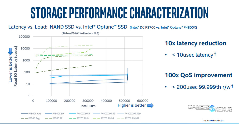
Latency Under Load
Technically, end users could purchase these data center drives – though we don’t recommend it at this time. The drives are supposed to deliver on low latency and high endurance. One of the more interesting combinations of numbers related to latency is latency under load. The drives are reportedly averaging <10µs latency on typical reads and writes, and Intel has information showing the drives performing 2GB/s write workloads with no problem. Let’s combine those two numbers. What an Optane SSD can do that “normal” SSDs can’t is withstand increased write loads while keeping read latencies about the same. In their tests – which should be taken with a grain of salt, of course – Intel says “read response times remained below <30μs while withstanding up to 2GB/s of random write pressure.” In comparison, a NAND Flash-based SSD like the Intel P3700 has an average latency of 100µs, several times slower than average Optane SSDs. When a NAND drive goes under write loads, its read latencies increase significantly. Because most users perform a combination of reads and writes (70/30 is a fairly safe ballpark), testing strictly for one metric at a time, while useful for baseline and review foundations, is not necessarily all that representative of use. A real-world example of where latency under load matters is paging. Games and operating systems have migrated away from paging as much as possible over the last decade because of slow storage performance, but with the low latencies promised by Optane. there wouldn’t be any real hit for paging.
Endurance
Another area of interest for storage heavy users is endurance. A fast drive with little endurance results in a quickly dead drive. Most enthusiast-grade drives today will outlive the usable life of the system by a longshot, but in the mind of an ever-cluttered digital storage space, users have an expectation of eternal data life. According to Intel’s numbers, the Optane SSDs are supposed to be have a lifetime of 12.3PBW. More impressively, the drives are listed to sustain a full 30 drive writes per day. Even if you could burn through that much data daily, your drive would still last you over a thousand days at maximum usage, beating out most currently available storage solutions.
Intel’s Testing Scenarios
Intel had a demo room with some preconfigured systems running various demonstrations. The most compelling involved a U.2 connected Optane SSD versus a U.2 connected Intel 750 SSD. Both systems were being used for rendering a SideFX Houdini demo called Maelstrom. The render is ~7 seconds (168 frames @ 24fps) of 1.1 billion particles all interacting with one another. What’s nice about this complex render is that it quickly exhausts the system memory, thereby forcing the machine to use swap space. The swap space was configured in Ubuntu 16.04 LTS with no special drivers installed on either system. Both machines were using the default NVMe driver to control the drives. Both systems were using X99 chipsets, 64GB of RAM, and 16-threaded CPUs. The end result was the compelling part: Intel 750@17hours, Optane@6 hours to render. Of course, this is a very specific use case, so we’ll have to see how that performance scales to other tasks.
Bringing Back U.2
Some readers may remember the U.2 connector appearing on motherboards in early 2016, then quickly fading away as the M.2 slot became the NVMe connection of choice. With Optane SSDs, Intel plans to re-emphasize the U.2 interface, making it the primary connection type for the SSDs. We now have a better understanding of why Intel pushed for U.2 a year ago on enthusiast motherboards, since Optane has apparently been in the pipeline for 10+ years.
Intel Optane Consumer Products
Very few enthusiasts will be willing to fork over the $1520 or $1951 required for a 375GB DC P4800X, and we’d strongly recommend holding any purchases or preorders until some reviews have gone live. This is a new architecture and is completely untested in the market. It’s arguable how much actual system responsiveness will be impacted by any iteration of Optan, and we’ll have to wait to test the thing hands-on to say more. If you’re interested in the Optane technology, wait just a little bit longer. Sometime in the future, Intel will likely make an announcement about a consumer drive that will likely be more budget conscious and client oriented.
Editorial: Patrick Stone
Video: Steve Burke