After completing all of our gaming, power, thermal, and other benchmarks for the new nVidia Titan V graphics card, we took the unit apart for cooler, PCB, and VRM analysis. We’ll be joined by overclocker ‘Buildzoid’ in the next few days for the advanced overclocking analysis of the PCB and VRM, but have some immediate information on the assembly of the Titan V and its cooler.
The card follows the same screw pattern as all previous nVidia Founders Edition cards, including the Titan Xp and GTX 1080, primarily isolating its cooler and shroud into a single, separable unit. Build materials are all the same, assembly is the same, but the underlying GPU, HBM2, VRM, and heatsink are different.
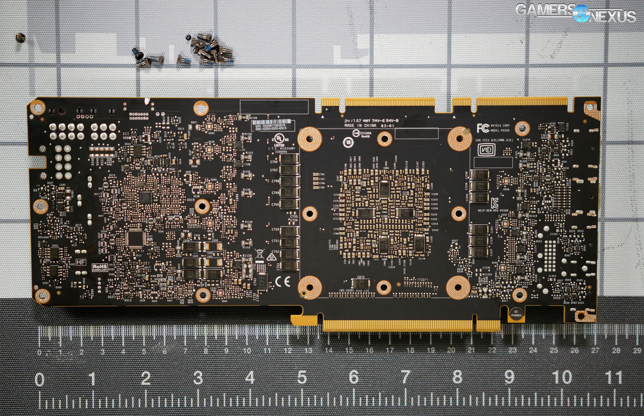
The backplate fastens into 4mm hex screws on the rear of the PCB, which then mount to the underside of the cooling baseplate. For the Titan V, nVidia’s baseplate only has some modifications versus previous reference coolers. The modifications accommodate new MOSFET placement, capacitor bank placement, and inductor positioning. Each MOSFET (and several inductors) is met with a protruded aluminum plate to sink more directly into the baseplate, with a canvas thermal pad resting between the two. The VRM on this board is a 16-phase built of Fairchild MOSFETs, with voltage controllers of somewhat ambiguous specifications – some of the controllers are by Monolithic Power Systems and have no public data sheets available, making it difficult to diagnose. We are working to probe the MOSFETs for more information on the wiring of the board, and will discuss that in upcoming content.

The cooler is changed only in a few locations, with new chamfered edges and beveled-up, mini finstacks toward the flanks of the cooler. It’s still a vapor chamber cooler, just with a wider baseplate protrusion for contact with the large die area. Speaking of, the contact zone is comprised of the GPU and four stacks of HBM2, which interface via 3072-bit bus. NVidia is using an epoxy resin coating around its HBM2, GPU, and interposer, which helps to protect the fragile interposer from uneven contact or user error during thermal paste clean-up. This resin extends to the outer edges of the silicon.

You’ll notice that SLI isn’t present, but that NVLink remains a physical option. As we understand it presently, NVLink is not yet functional, but is on the board.
We’re working to analyze the PCB and VRM now. Our first round of benchmarks will also hit the web shortly.
Editorial: Steve Burke
Video: Andrew Coleman