AMD’s technical press event bore information for both AMD Ryzen and AMD Navi, including overclocking information for Ryzen, Navi base, boost, and average clocks, architectural information and block diagrams, product-level specifications, and extreme overclocking information for Ryzen with liquid nitrogen. We understand both lines better now than before and can brief you on what AMD is working on. We’ll start with Navi specs, die size, and top-level architectural information, then move on to Ryzen. AMD also talked about ray tracing during its tech day, throwing some casual shade at NVIDIA in so doing, and we’ll also cover that here.
First, note that AMD did not give pricing to the press ahead of its livestream at E3, so this content will be live right around when the prices are announced. We’ll try to update with pricing information as soon as we see it, although we anticipate our video’s comments section will have the information immediately. UPDATE: Prices are $450 for the RX 5700 XT, $380 for the RX 5700.
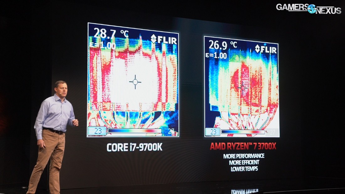
AMD’s press event yielded a ton of interesting, useful information, especially on the architecture side. There was some marketing screwery in there, but a surprisingly low amount for this type of event. The biggest example was taking a thermographic image of two heatsinks to try and show comparative CPU temperature, even though the range was 23 to 27 degrees, which makes the delta look astronomically large despite being in common measurement error. Also, the heatsink actually should be hot because that means it’s working, and taking a thermographic image of a shiny metal object means you’re more showing reflected room temperature or encountering issues with emissivity, and ultimately they should just be showing junction temperature, anyway. This was our only major gripe with the event -- otherwise, the information was technical, detailed, and generally free of marketing BS. Not completely free of it, but mostly. The biggest issue with the comparison was the 28-degree result that exited the already silly 23-27 degree range, making it look like 28 degrees was somehow massively overheating.
Let’s start with the GPU side.
GPU Specs, Frequency, Die Size
AMD has two GPUs it plans to release in July of 2019, with exact date TBD at time of filming. Ryzen 3000 mostly launches on July 7th, so the GPUs will push around the same time. The two cards will be the RX 5700 XT and RX 5700 non-XT, both moving away from GCN and toward the new RDNA architecture. We’ve known GCN to be extremely limited in cache bandwidth and in scalability past 56 CUs, so RDNA will be a refreshing change that should be interesting to study. GCN will stay alive for the high-performance deep learning and non-gaming market segments, but RDNA will be the gaming architecture going forward.

The RX 5700 XT will host 40 compute units with 64 stream processors per CU, or 2560 SPs for the 40 CU RX 5700 XT. This is the same SP per CU count as Vega 10, also at 64 stream processors per CU, but note that you can’t linearly compare the streaming processors 1:1. In an AMD performance demo, the company showed to press that its Navi 10 GPU – that’s the one used in the 5700 series – posts about 14% higher performance versus Vega 56 with about 23% lower power consumption. This was an AMD internal demo, so we obviously need to validate at homebase, but that uplift is promising for RDNA’s significantly smaller first GPU. Speeds were listed to media as 1905MHz boost, 1755MHz for gaming workloads, and 1605MHz base. The delta between boost and gaming tells us that AMD’s chosen blower cooler was once again a poor decision, to no one’s surprise, as there should be more thermal and power headroom to clock higher for gaming workloads if using a proper cooler. We’ll talk about the negatives more later, let’s get back to specs and positives first.
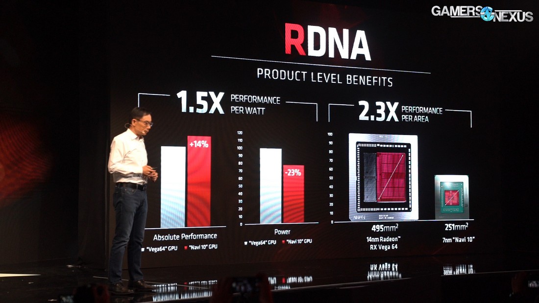
As for GPU size, AMD also provided that information to press. The Vega 64 die measured at 495mm^2, with Navi 10 measuring at 251mm^2. This is important, and it’s for a lot of reasons: By significantly cutting the die size, and also by eliminating the highly expensive HBM2, AMD is able to cut its manufacturing cost significantly and finally start competing with NVIDIA directly in price. AMD claims its RX 5700 XT will be the direct RTX 2070 competitor.
Either way, we know for fact that Navi 10 GPU and GDDR6 costs will be lower than Vega 10 and HBM2; furthermore, if AMD’s claims of increased performance per watt with increased performance per area prove true, Navi may be a re-entry into the gaming market. We still want to see a flagship AMD card – AMD hasn’t had a true head-to-head top-end competitor with NVIDIA for a while, with Radeon VII being the closest but still falling short. A flagship class card is needed for halo marketing so that sales cascade down the stack, but for now, it looks like another mid-range foray by AMD, it’s just that this one is more promising than the refreshes and power-hungry brutes we’ve seen in the past. We’d advise, as always, tempering hype until we can see third-party benchmarks and numbers.
In short, the RX 5700 XT has 40 CUs, 8GB GDDR6 at 14Gbps for 448GB/s bandwidth, 1755MHz gaming frequencies, and 1905MHz boost, likely limited by the blower cooler. We’ll have to see what better solutions can do with more serious overclocks at a later date.
The RX 5700 non-XT will cut down to 36 CUs and 2304 stream processors, with an 8GB GDDR6 framebuffer and GPU speeds of 1725MHz boost, 1625MHz “gaming,” and 1465MHz base.

AMD was forced to acknowledge real-time ray tracing this time, but doesn’t have immediate support plans. From our end, we think this is fine, and that the market demand for real-time ray tracing features is low enough to be mostly irrelevant. That didn’t stop AMD from casting stones at NVIDIA, though. AMD mostly took the easy jabs, like its stated goal to “drive ecosystem so that gamers can take full advantage of the features they pay for.” Other digs included references to delayed uptake on RTX features. AMD is looking at support in the future, but isn’t immediately worried with real-time ray tracing support.
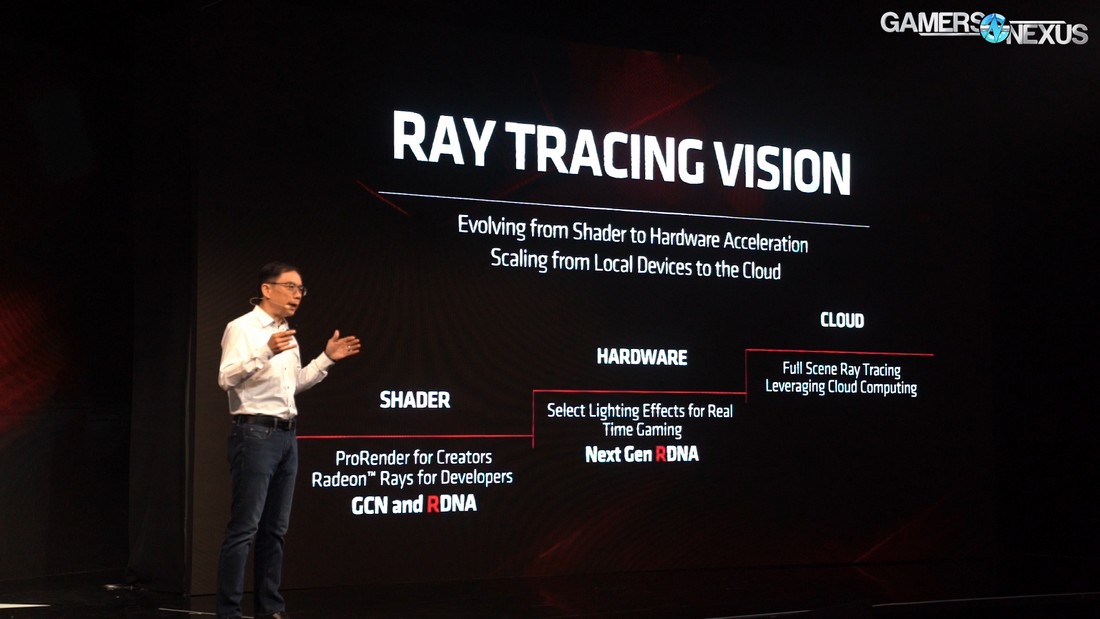
As a quick aside, note that AMD is planning a 7nm+ Navi GPU for late 2020 or 2021, and that it is aiming to support some form of hybrid ray-tracing in the future.
RX 5700 XT & 5700 New Overclocking Limits
Total board power should be 225W for the 5700 XT and 180W for the 5700 non-XT. We asked if VBIOS would be locked and, due to security concerns, AMD is locking down custom VBIOS modifications. We then asked if powerplay table hacks will still work this generation, but we were told that we’d have to learn new tricks to bypass the power limits. That’s a little bit of a let-down from the fringe use case of power modding, but we’re hopeful that we can find new power bypasses.
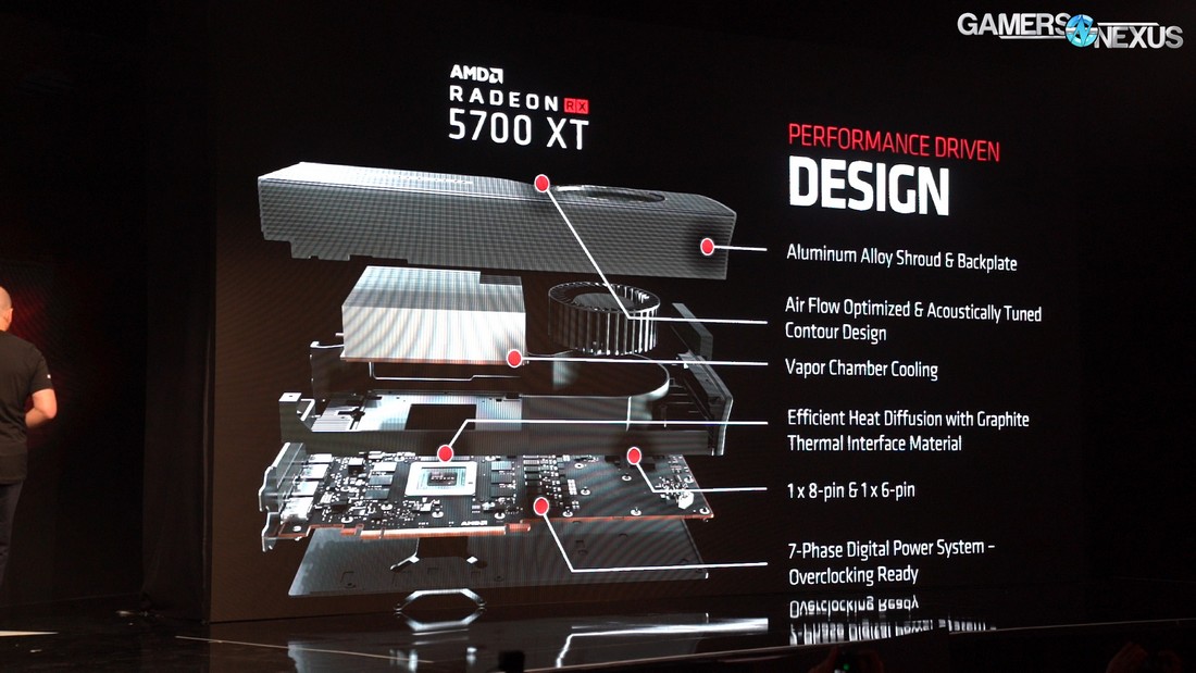
The reference card is a blower cooler with a vapor chamber, a design we’ve seen struggle in the past, and AMD claims to be listening to feedback. Unfortunately, the company still went with a blower cooler, but it has listened to some parts of criticism. One of those was noise levels, where AMD is now capping its noise level to 43dBA, although we don’t know at what distance that noise was measured. We do know previous cards stretched upwards of 59dBA with a 20” measurement.
The reference 5700 XT PCB has a 7-phase VRM. AMD couldn’t answer questions about what power stages were used, so that information doesn’t mean anything right now, but we did learn that the 5700 XT should be a 6+1 layout and that the 5700 should be 5+1. We also noticed that the cards don’t have a VBIOS switch, but we’re not sure if that’ll change for the full retail product. It probably will be single VBIOS.
Ryzen 3000 Memory OC, XOC 16-Core, PCIe Gen
Before diving deeper, let’s take a break from GPUs to talk CPUs. On the CPU side of things, we learned that AMD was hitting 5.35GHz all-core on the 16-core CPU with liquid nitrogen when using an MSI Godlike motherboard; this matches what we heard previously, and as a reminder, we also had a motherboard manufacturer at Computex tell us they were hitting 5.5GHz and trying to approach 6GHz on the 12-core CPU. Critically, overclockers will no longer have to step down to PCIe Gen1 for benching and can run full PCIe Gen3 or Gen4. Cold bugs will depend on the CPU, and AMD was running its XOC at about -150 degrees Celsius.
For memory overclocking, Ryzen 3000 is supposed to fairly easily support 3600MHz XMP without issue, and we’ve also seen clocks on MSI boards up to 5100MHz with timings at 18-21-21-56-1T. That 5100MHz overclock was done with air cooling on the CPU and is a result of better trace layout and a new controller design.
Ryzen 3000 Architectural & Gaming Improvements
Some of the more noteworthy architectural changes to Ryzen 3000 CPUs focus on higher IPC and higher gaming performance. Interestingly, in AMD’s engineering discussion, the senior architects and AMD fellows thought Zen2 would see frequencies regressing. Engineers originally thought the jump to 7nm would result in lower clocks, relegating Zen2 to a server part. The team was able to figure it out, though, and managed to boost frequencies overall.
Key changes included the following:
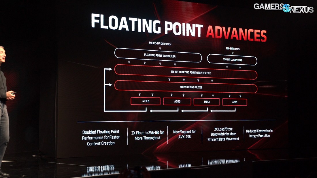
- AMD doubled the size of the floating point engine to 256-bit, which means AVX-256 can now run single-cycle on Zen2, so that’s a big change
- AMD has doubled its load/store bandwidth for data storage and movement
- Integer execution was also improved, primarily by reducing resource contention during integer operations
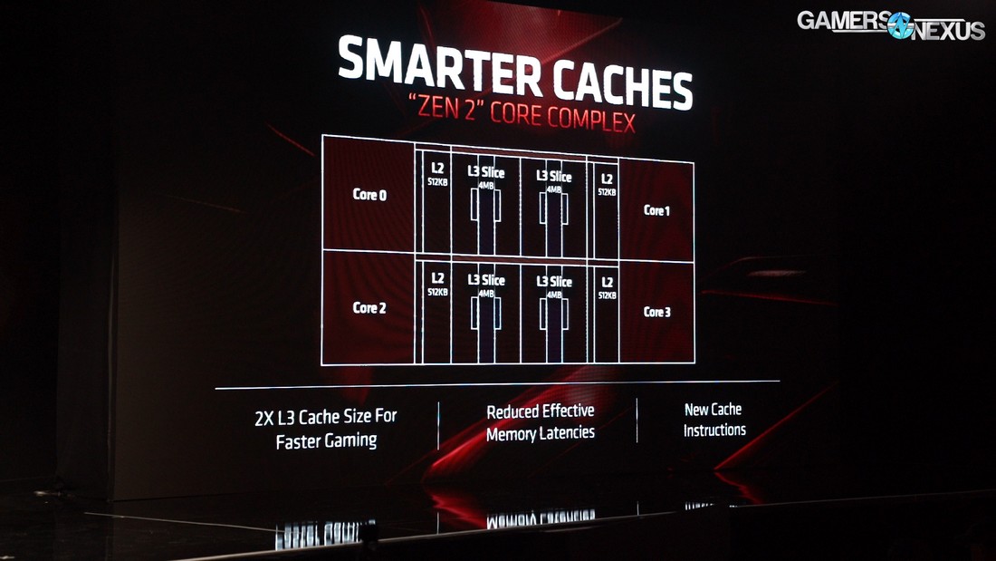
AMD also doubled the L3 cache size. More data in local cache means fewer hits to memory, but also reduced effective latency to system memory. AMD further highlighted that improvement in prefetching algorithms further reduces the effective memory latency. As an aside, AMD has made the unfortunate decision to rebrand L3 cache as “Game Cache,” so if you see that name in the future, that’s what it means.
AMD showed some more internal benchmark charts, and while we know there is improvement in gaming, we’d again advise to wait for our own benchmark testing. Most of the internal charts looked GPU-constrained, for instance, and so we will not be reproducing them here as we believe them to be misleading. We do anticipate performance uplift if only from the IPC and frequency jump, both of which will have direct impact. Memory is also more easily tuned to 3600MHz and beyond now, as mentioned in the OC section.
AMD also walked through architectural changes that we’ll speak to in more depth approaching launch. For some quick stats, we learned that AMD has moved its integer execution to a 92-entry integer scheduler from 84 previously, it has increased physical register file entries from 168 to 180, grown the reorder buffer from 192 to 224, which is meant to help with making-up for the latency hit by increasing L3 size, and AMD has increased the store queue from 44 to 48, with increased load/store bandwidth by 2x.
We have a lot more to talk about in this storyline. AMD gave us multiple pages of additional notes on architecture, product information, and software, and we’ll be digging through this incrementally over the next few days. For now, this content pieces will get us started. The RX 5700 XT and RX 5700 pricing will both be added to this content as we receive them, just note there may be a latency as we’ll be on planes home around when the AMD stream goes live. Note also that we’ll be keeping an eye out for more 3950X news from AMD.
More to come. We're flying back home, so we'll write-out the rest on the plane.
Editorial, Host: Steve Burke
Video: Keegan Gallick