NVIDIA GTC 2020 Keynote Recap: Ampere A100 GPU Specs, Ray Tracing, DGX-3, & EGX
Posted on
Linus might have competition from NVIDIA CEO Jensen Huang, who today published the GTC 2020 keynote from his kitchen, given the current world circumstances. The company’s GTC event has rarely featured gaming product launches over the last few years, but often features the architectures that lead into them. Volta is a good example of this, where we didn’t really get gaming cards, but we saw what led to Turing. At this year’s event, the company showed off its new Ampere architecture, with a split-focus on reminding us of gaming and ray tracing advancements while also highlighting all the usual AI, machine learning, and deep learning processing goals of the architecture. Ampere sounds like it’ll be coming down to gaming at some point, as opposed to the Volta/Turing relationship, where they were technically different architectures and launches.
We thought NVIDIA might livestream a pre-recorded video, but the company ended up uploading multiple edited videos into at least 8 parts at time of writing (ed: ended up being 9). Admittedly, some of them were a little hard to listen to with obvious cuts and shoved-in words, but we’re probably more sensitive to that than most since we make so many videos here and deal with that weekly.
This article is a direct paste from our video script due to tight timelines on turning content around for news.
RTX & DLSS 2.0
There wasn’t a lot of RTX news, but there was some. The company reminded everyone of DLSS and its existence, and showed off DLSS 2.0 again. Huang acknowledged that, quote, “most people didn’t think this would work,” and said that the “first generation was a little blurry,” then showed DLSS 2.0 images by comparison and claimed that DLSS 2.0 did a better job than 1080p native,” we’d assume talking about 720p with DLSS.
Regarding RTX and ray tracing products, it was mostly re-emphasis that the product stack exists, with some gloating about “when we launched, people were skeptical, but now it’s here.” To be fair, when it launched, cards were dying left-and-right with artifacting defects and there weren’t any RTX games for about 55 days after launch of the card with the same name, so people were rightfully skeptical. That said, NVIDIA has completely shifted the focus of the industry to ray tracing, and has done so earlier than probably the rest of the industry was ready for -- like AMD -- and so now everyone is rushing to build around it. We’ll give them credit on that. Even the new consoles are talking ray tracing.
NVIDIA Omniverse

NVIDIA also talked about its Omniverse solution, which is an RTX server filled with RTX 8000s. None of this features new GPU architecture, but the company did show-off a fully playable physics-based ball mechanic game (similar to classics, like Spectraball). Camera movements were somewhat nauseating to watch, but the graphics were the focal point.
NVIDIA Ampere
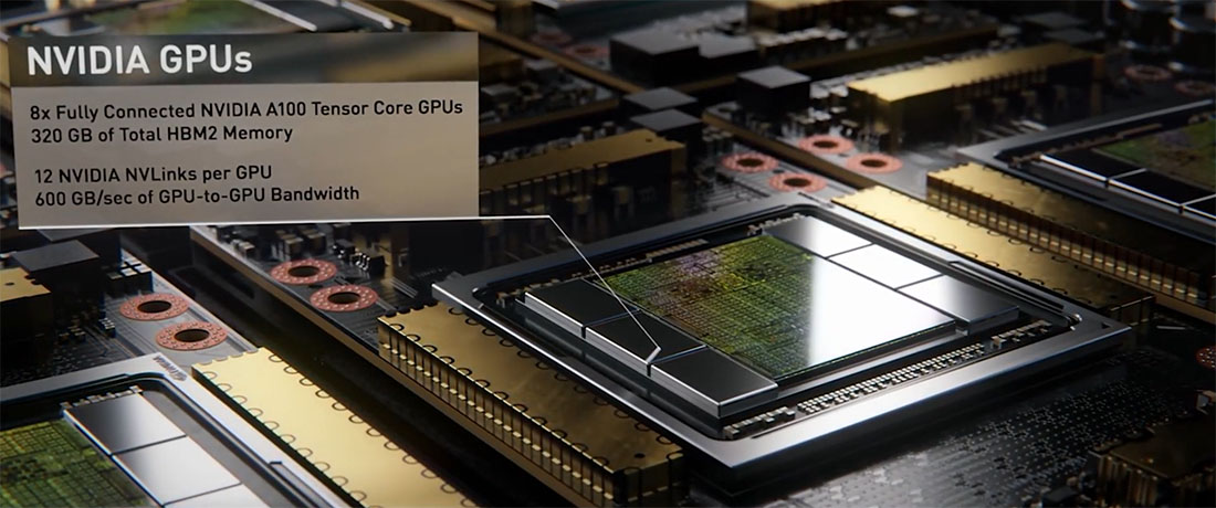
NVIDIA did its usual “World’s Largest GPU” announcement as well, featuring NVIDIA Ampere and the A100 processor board. This is built for data center and enterprise use, and isn’t a gaming product, but is something that will eventually feed into gaming products. It’s also worth covering just because it is a major advancement in its space.
Most people by now have seen the clip of Huang pulling the board out of his oven. We learned more about that board in today’s video keynote: The A100 processor board weighs 50 pounds, hosts 8 GPUs via the new NVLink 600GB/s interface, and has 6 switches. Some additional interesting facts that were just for fun include the 1 kilometer of copper traces connecting all the hardware and the 1 million drill holes to hold it all together. That last fact isn’t much of a surprise, given how much NVIDIA likes its screws in RTX cards. NVIDIA also noted that it’s comprised of over 30,000 components, so those were some busy SMT lines, and that it has, quote, “the most transistors on one computer” ever made.
NVIDIA’s Ampere announcement also featured a new “MIG” architecture, or multi-instance GPUs for “elastic GPU computing.” After using a somewhat strained rocketship analogy, Huang explained that MIG allows each A100 GPU to be split into 1 whole instance, as most cards are used now, or into 7 instances for isolated applications or isolated users. For data center, the implication here is that you could now sell down-costed access to less computing hardware for applications that don’t need as much horsepower, but not require a standalone GPU to host that lower-cost user. They’re just a sub-user on a card, so if you’re Amazon, you may end up selling 6 instances to a major AI company and one instance to a university student, as an example, and still run everyone on a single A100 board.
Ampere’s focus is on inference and training, with the partitioning into smaller GPUs seemingly its primary selling point outside of the speed advances. NVIDIA says that data centers can be architected such that smaller GPU partitions are used for “scale-out” applications, or larger GPU instances can be used for “scale-up” applications.
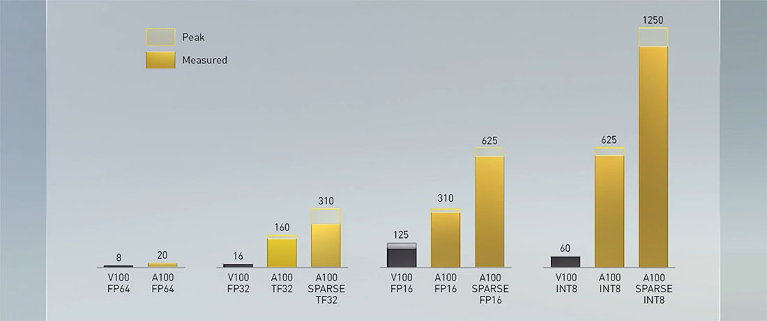
For those in our audience who may do more with artificial intelligence, deep learning, or machine learning, we’ll go through the stats that NVIDIA presented:
NVIDIA’s performance slide only had data labels for peak performance, but most of the peaks were close to the sustained average, and at GamersNexus, we admittedly aren’t even sure what most researchers using this card look for in specs anyway. It’s not our coverage area. For the numbers given, NVIDIA claims that A100 FP64 double-precision performance is 20 TFLOPs, versus 8 TFLOPs on V100 Volta with FP64. Assuming the same approach to measurement, that’s obviously a big jump, but how that translates to real-world performance will hinge on the application. Gaming certainly doesn’t get a linear TFLOPS translation to FPS or frametimes, but this is out of our coverage area. The Tensor Float performance was listed as 16 TFLOPs on the V100 for FP32 tensor float, 160TFLOPs on the A100, and sparse data optimization at 310 TFLOPs peak for FP32 tensor float.
For FP16, NVIDIA noted the A100’s spare data performance at 625, its non-spare performance at 310 TFLOPs, and V100 at 125. NVIDIA separately noted that most people use FP32 fo their work in this space, and so its focus is on FP32 and not FP16.
INT8 performance has NVIDIA claiming that the A100 is, quote, “the first processor over 1 petaflop,” marking the A100 at 1250 TFLOPs peak for sparse, 625 peak for non-sparse, and using the V100 at 60 TFLOPs for INT8 as a reference point.
NVIDIA used a speech recognition demo to identify birds based on the sounds made, primarily using this as an example of how the instances process data when split or combined on the A100 cards. With all 7 MIGs working as a single GPU, NVIDIA noted 500 queries per second, whereas it compared this to Volta’s 80 per second.
DGX
The next major announcement was DGX, which is NVIDIA’s mini-supercomputer it sells to business clients. We’ve actually seen parts of the definitely-not-DGX being made at definitely-not-Cooler Master, and the new one is using the same gold mesh faceplate as the previous generation.
NVIDIA’s new DGX A100 solution is the third generation of the DGX line, and NVIDIA says it has been optimized for “training, data analytics, and inference.” Because the DGX has 8 of the NVIDIA A100 GPUs, it can be instanced for up to 56 simultaneous users, or can used as 8 GPUs. The machine has 9 Mellanox CX6 interconnects, with each NIC at 200Gbps. Mellanox is a company that NVIDIA acquired recently, so this inclusion was predictable. For CPUs, NVIDIA tapped AMD’s 64-core Epyc Rome processors, running two Rome CPUs at 128 cores total for each DGX box, including 1TB of memory between them.
The new NVLink also makes an appearance at 600GB/s, but we need to note that this is explicitly different from NVLink on the gaming cards. There is a slower, cut-down version for gaming, while the 600GB/s solution found here is much more expensive and also targets a much heavier workload than found in gaming multi-GPU applications. We probably won’t see a 600GB/s NVLink bridge for SLI.
Other specs on DGX include 15TB of PCIe Gen4 NVMe SSD storage and 4.8TB/s of bi-directional bandwidth.
The DGX will cost $199,000, making it actually comparatively cheap to previous DGX solutions when given its processing capabilities. If you felt buyer’s remorse from the 2070 Super launch after buying the RTX 2080, imagine buying a $400,000 mini-supercomputer and hearing the new one is $200,000.
These advancements are all noteworthy for the clientele targeted, and one of the more appreciable differences to anyone interested in reduction of land development is the significant decrease in space required for datacenters with higher-performance computers. Of course, with cost coming down, the more likely end result is that developers will either run less optimized code against higher horsepower hardware or they’ll just find other uses for it. Ideally, we’d see a scaling down of space developed, though.
NVIDIA gave an example of a 25-rack AI data center priced at $11m and requiring 630kW to run, noting it had 50 DGX-1 systems for training and 600 CPU systems for inference. That’s the original DGX, mind you, so it’s two generations back from this one.
The newest DGX A100 solution would be a $1 million deployment for 1 rack at 28kW, with a major space reduction. NVIDIA used the PageRank algorithm and the common crawl data set to test the performance of these two, noting 2.6TB of data and 128 billion edges for a small fraction of the internet.
NVIDIA said that it usually takes 3000 servers and 105 racks to analyze 52 billion edges per second, versus four DGX A100s via NVLink (for one giant DGX) to process 688 billion edges per second. Huang then made the usual “the more you buy, the more you save comment,” and his laugh indicated that he’s in on the joke.
NVIDIA Edge AI
NVIDIA also announced its NVIDIA EGX A100 solution, which seems to have a heavy focus on security and authenticated boot solutions for IOT.
The EGX has a Mellanox ConnectX 6 network solution mounted to the card, at 100Gb/s ethernet or infiniband on-board. The two together are what differentiate this as an “EGX” device. NVIDIA noted that its focus on automation advancement and training, and highlighted a partnership with BMW and EGX. NVIDIA says that BMW builds 40 car models with 100 options every day, imports 30 million raw parts from 2000 suppliers, and sends those parts to 30 factories worldwide. Huang said that BMW can assemble one car every 56 seconds, which is insane for a number of other reasons, and referenced just-in-time manufacturing where new crates of parts are dropped off as old crates leave. Robotics is involved in all of this, and NVIDIA is working with BMW on training future robotics deployments.
Editorial, video: Steve Burke