Graphics manufacturer AMD and its Radeon Technologies Group (RTG) today announced the arrival of “Polaris,” a 14nm FinFET architecture derived from codename Arctic Islands. Polaris is due in mid-2016 and supersedes the aged 28nm process, which both major GPU manufacturers presently employ. The new node should drastically impact performance-per-watt, aided by FinFET transistors (shaped like a 'fin,' rather than planar, so containment of power is more efficient – i.e., less leakage).
AMD's initial slide deck demarcates a move to an updated GCN CU architecture (4th generation), a new geometry processor, updated display engine, command processor, L2 Cache, and memory controller.
The geometry processor is of high interest to us. In recent game benchmarks, we've seen AMD devices struggle with geometric complexity in some game environments, something that may be improved with focused updates specifically on geometry processing. Tessellation processing is also a weak point for AMD, though we're presently lacking any details pertaining to real tessellation performance expectations for Polaris.
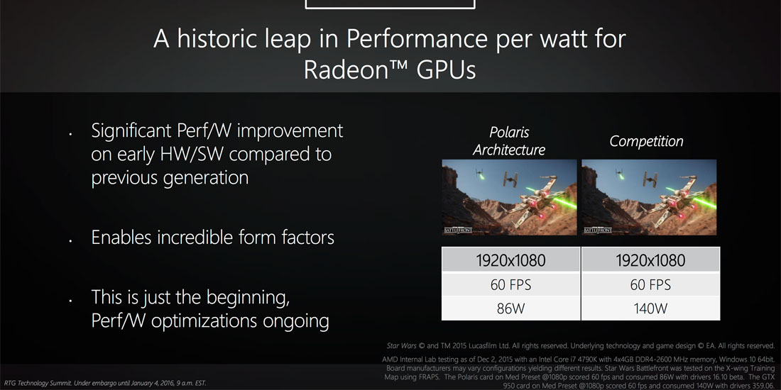
AMD's slide deck shows a few initial benchmarks, indicative of 85W power draw under Battlefront load. Those initial benchmarks, when looking at the fine print, were executed at 1080p / medium in a game which isn't particularly graphics intensive to begin with. A decent starting point for comparison, but certainly nothing to print as end-all TDP fact just yet. Gaming performance metrics are not yet available in a usable capacity.
Display interfaces are also being updated on Polaris, moving to HDMI 2.0a, DisplayPort 1.3, and enabling high bitrate encode/decode through 4K h.265.
Currently available details are minor, but we're scheduled to meet with AMD at CES this week and hope to learn more.
- Steve "Lelldorianx" Burke.