When you really start getting elbow-deep into PC building and specs -- much deeper than our recent budget PC builds have gone -- it's easy to get overwhelmed by all the acronyms and terminology used by white papers and specification sheets. Our previous video card guide looked at the pros and cons of AMD vs. NVIDIA for gaming, but this one is (relatively) universal and can be applied to almost all aspects of graphics processing technology. This "GPU Dictionary" explains the difference between memory clocks and core clocks, shader specs, what a ROP is, and some other basic (and fun) GPU phrases.

Similar to our surprisingly in-depth case fan guide, this GPU dictionary is outlined in such a way that it will retain relevance through time, so - for the most part - you won't have to worry about re-learning anything.
Common Specifications
This section is dedicated to the specs that you'll find listed on retail websites (particularly Newegg), giving you a top-level look at the basics of video card terminology.
Interface: The 'interface' largely determines whether a card is compatible with a motherboard or not. You'll want to try to match the video card's interface with that of the motherboard's expansion slots, although there is a lot of inter-compatibility.
Here's a list of modern interfaces (we've neglected deprecated technology as it is, other than for historic purposes, no longer relevant):
- PCI Express 2.0: PCI Express (see also: PCI-e) took the world by force nearly a decade ago, blowing AGP out of the water with its expanded bandwidth. PCI Express 2.0 still serves as a standard, although newer interfaces will be replacing it shortly. Video cards that operate on a PCI-e 2.0 interface are inter-compatible with PCI-e 2.1 and PCI-e 3.0 slots (2.1 and 3.0 are backwards-compatible). The "x" number primarily symbolizes the number of available lanes (effectively the bandwidth limiter); x4 is 4 lanes, x8 is 8 lanes, x16 is 16 lanes, and so on. The number of lanes acts as a modifier to the transfer bandwidth, we've made a simple graphic to explain it:
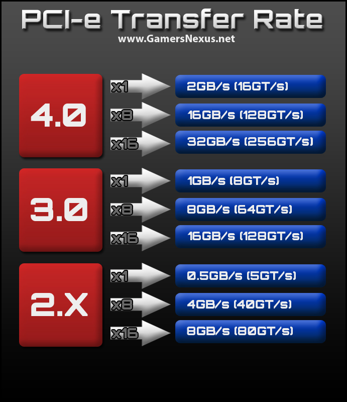
- PCI Express 2.1: 2.1 is no faster than PCI-e 2.0; there's almost no difference between PCI Express 2.0 and 2.1 other than additional instruction sets and debugging/troubleshooting support that are available on 2.1. This was mainly in preparation for the migration to 3.0 and has no impact on gaming.
- PCI Express 3.0: With the 7970's release comes the first officially-supported PCI-e 3.0 video card, and with that comes much scrutiny. As noted in our image above, PCI-e 3.0 x16 slots allow for massive bandwidth increases over PCI-e 2.x (an impressive 100% increase). Since most modern cards do not even come close to using the full PCI-e 2.0 x16 bandwidth when gaming (perhaps when computing), the advancement is currently of limited advantage for gamers. In short: Don't go out of your way for PCI-e 3.0 until GPUs have progressed to a point of utilizing the full bandwidth for gaming (this also depends on video game programming). Nvidia's predicted 1000% increase in computing power will allow for many advancements in gaming graphics, though, like ray-tracing, better HDR, bloom, smoke, and atmospheric effects to be rendered effectively in real-time, which is when we'll start seeing that bandwidth utilized more efficiently.
GPU: The GPU itself, despite being interchanged with 'video card' or 'graphics card' frequently, is not identical to either of those. Video card and graphics card refer to the entire unit, whereas GPU (graphics processing unit) refers specifically to the processor that is buried under that massive video card heatsink. GPUs are incredibly powerful microprocessors that are optimized for graphics computations and rendering.
Revision: You might see this come up in GPU-Z or other specification reading programs. You probably already know what this is: it's the iteration of GPU that you're running. In hardware development, there are two types of "revs" (or revisions): X-revs and A-revs. X-revs are the development or prototype iterations, while A-revs are "production" versions. A higher number signifies a later iteration. Most cards will be rev A1.
Advanced Specifications
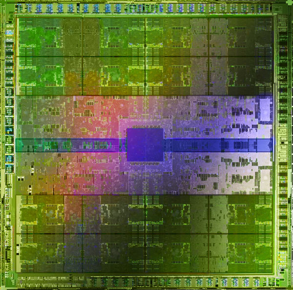
Die: In computing, "die" is used to refer to the bare piece of silicon of which the processing unit (a GPU or CPU) is comprised. Die is often interchanged with "chip." Here's a diagram of the die for nVidia's Fermi architecture:
Die Size: You'll see this number come up in programs like GPU-Z. This is the physical size of the die (as explained above). For example, the die size of my GTX 580 is 520mm2.
Architecture: GPU architecture describes the platform or technology upon which the graphics processor is established. New architecture is implemented relatively infrequently - on average, every two years or so - and has broad affects on the GPUs capabilities and performance. Architectural advancements in computing are unbelievably important: They allow us to decrease overall size of the technology which, in turn, crams more features and transistors onto a single die (improving performance).
Memory Bandwidth: This is one of the single, most important aspects of graphics processors. Memory bandwidth determines your card's ability to utilize its onboard video RAM efficiently when under stress. Think of it like the lanes on a highway: if you have a highway with 3 lanes that is perpetually congested, then you add 3 more lanes to it over the weekend, you'll see a significant decrease in traffic (if not outright elimination of congestion). The same is true for GPUs: having tons of GDDR5+ memory won't do any good if the pipe is too small to use it in time.
Memory bandwidth is calculated by memory type (i.e., GDDR5, GDDR4, etc.), the memory clock, and the actual memory width. Calculate the maximum memory bandwidth by multiplying the memory clock by the memory width and the transfers-per-clock of the memory type.
Core Clock: The frequency at which the GPU is running. This can be sort of compared to a CPU's operating frequency. "Speed" depends on numerous factors, architecture being one of them. It's not necessarily an apples-to-apples comparison to look at the core clock speed of an older GPU and a newer one (or cross-brand differences), but for sake of ease, greater core frequencies equates faster computing. Be careful with that, though, calculating speed in gaming is never quite so linear.
Memory Clock: Quite simply, this is the speed of the video card's onboard memory. As above, the memory clock helps calculate memory bandwidth; a higher memory bandwidth equates better performance for anti-aliasing and other memory-intensive tasks.
Memory Interface: This is the memory's actual bus width, typically in the form of 128-bit, 256-bit, or 384-bit. The memory interface is used to calculate total bandwidth. A bigger interface means a bigger pipe. A smaller interface can be compensated for by faster memory clock speeds or different types of memory.
3D API: DirectX and OpenGL are used for game graphics interpretation. At the time of this article, DirectX 11 is the most recent variation of the DirectX heritage, giving better ambient occlusion and dynamic lighting than its Dx10 predecessor. When shopping for a GPU, you'll want to cross-check with the most recent version of Dx and see if your preferred cards match with it. Check what the newest additions to that version of Dx are to see what you may be gaining or missing out on.
RAMDAC: Random Access Memory Digital-to-Analog Converter - but what does that mean? As the name might suggest, RAMDAC is responsible for converting digital-to-analog signals. The transfer rate of RAMDAC helps determine the maximum supported refresh rate of the video card; that said, non-analog outputs (DVI, HDMI) do not even necessarily require RAMDAC, while VGA and SCART do. Since analog signals are rapidly becoming obsolete and deprecated, RAMDAC has become a standardized, uninteresting component of modern GPUs.
ROPs: Render Output Unit(s) or Raster Operations Pipeline. A ROP handles pixel output and arranges the pixels on your screen, as well as basic rendering tasks. ROPs deal heavily with multisample anti-aliasing by manipulating pixel color in a way that enhances previously-rendered geometry to look significantly better.
Shaders: The number of unified shaders impacts your ability to handle different shadowing and shading techniques when gaming or benchmarking. There are three primary shader types:
- Pixel Shaders: These are more primitive and supported by nearly all graphics processing units, even shoddy onboard ones. Pixel shaders process the simple color, specular highlighting, and bump-mapping, as well as depth handling. The pixel shader is not 'aware' of what's going on around it; it only knows what that single pixel it's working with is supposed to do. This limits its capabilities to be quite simplistic in terms of what we're used to.
- Vertex Shaders: Vertex Shaders calculate vertices' 3D locations and then correlate them with their relative 2D screen render coordinates.
- Geometry Shaders: These are much more complex and can handle advanced graphics calculations that are normally associated with gaming. Geometry shaders are executed last in the shader pipeline (after pixel and vertex shaders), but process more advanced stages of graphics, like tessellation, shadow extrusion, and real-time rendering tasks.
Texture Fillrate: Using GPU-Z to analyze my GTX 580's specs, I see that it has a pixel fillrate of 37.1GPixel/s and a texture fillrate of 49.4GTexel/s -- but what does that mean to the end-user? The Texture Fillrate is, simply put, the number of pixels (in this case, 49.4 Gigatexels) that are textured and rendered to the output screen per second. The process of "drawing" pixels to the screen and applying the appropriate textures to them is called texture mapping, and is handled by texture mapping units (you may have seen your card spec read how many "TMUs" it has -- that's what they're for).
Pixel Fillrate: Similar to the above, this is simply the per-second amount of pixels that your GPU can draw to the screen. Pixel fillrate is an aging spec and should have almost no impact on your purchases.
Let us know if we missed any! I'm working on expanding these "dictionary" articles constantly and can use your questions to add more definitions to them.
As always, let us know below in the comment or post on our hardware forums if you require further assistance!