From conception of design, to development, to evilly-scheming robots that (for now...) mount chips to PCBs, the process behind solid-state drive advancements can be months in the making. The controller alone can take a year (or more, in some cases) to finalize, and even then, it has to ship to manufacturers, get soldered to boards, and be tested, all prior to your consumption.
In this feature, we'll walk through the development of an SSD and its controller and explain how SSDs are made. Each major step of the process will be broken-down into core tasks and includes insight from industry experts. We also have some cool photos of SSD production facilities, found below.
This undertaking involved a good deal of interviews with those in the industry, so for brevity, we'll credit everyone in a list and then quote accordingly throughout the article:
- Kingston: Cameron Crandall, Technology Manager
- Kingston: David Leong, PR Manager
- Kingston: Danny Ordway, PR
- LSI/SF: Brian Garabedian, PR Manager
- LSI/SF: Kent Smith, Senior Director of Product Marketing
And finally, before starting, here are some links to previous articles that are relevant to this topic, which may prove useful to those researching SSDs:
- SSD Dictionary: Understanding SSD Specs
- Do You Need an SSD For Gaming?
- Kingston Interview
- Finding a Bottleneck in Your PC
What Goes into an SSD?
SSDs consist of a few key components - namely NAND Flash and the Flash Storage Processor (or "controller") - but time is the biggest element to factor into an SSD's development. SandForce alone -- which LSI acquired in January, 2012 -- employs approximately 150 engineers and developers for their SandForce Flash Storage Processors. It's a large industry with a lot of interconnected parts -- if one aspect slows down, it's quite possible that it could slow down other parts that are further down the chain, too; Kent Smith of LSI laid it out simply: "Everyone in the industry has to keep up with each other."
That time is broken down into several phases, and across the industry, the top-level phases are all fairly templated: Design, Development, Testing, and Production. Each of these layers spiders into differing sub-phases, depending on the company's primary function. Here's a simplified flowchart to help illustrate the time allotment per phase:

Note: Although there is an axiomatic directedness to the flow of development, none of these departments are ever sitting idle -- everyone is always working on something, even if it's updates to previously-launched firmware.
SSD Phases: Market Analysis and SSD Design
Linus Torvalds recently professed his love for SSD design (and also said to HDDs, "Get thee behind me, Satan!"), noting that the stability and low-TDP are necessary for his work. SSDs have grown in their feature-sets with each generation, with the goal of hopefully creating a faster, more accessible platform; these features are first discussed in the design phase.
Responsible for analyzing customer requests, business requirements, company objectives, performance and endurance specifications, and other desirable facets of the impending product launch, the design phase is where a company defines its goals and entertains feature requests; it's the very first step in a solid-state drive's life. In general, the design phase breaks into something like this:
- Marketing Requirements Document: The marketing team will draw-up what they think would make a successful and powerful product by assessing the current market environment.
- Engineering Response: Engineers reply with how much of this is feasible within a set amount of time using currently-available technology.
- Back & Forth: The company will decide internally which features can be tabled for later, which ones are immediately possible, and which ones must be developed. Those that need to be further developed will then be discussed with third-party, controller-only manufacturers and the SSD manufacturing team, depending on requirements.
- Product Requirements Document: This finalized document outlines the required hardware and firmware specifications for the SSD. Once this document is approved and everything is greenlit, the SSD manufacturer can then move on to the development phase.
The objective during the design phase is to determine what volatility or fluctuations in current market conditions are present, explore demands from customers, discuss adequacies and inadequacies of current options, and then hone-in on desirable and achievable features. If the feature is something that must be implemented on a Controller-level, SSD manufacturers can initiate dialogue between their selected controller provider (LSI SandForce, Indilinx, Marvell, Intel, etc.).
When Cameron Crandall, Senior Technology Manager at Kingston, delved into Kingston's SSD design/dev process for us, he explained the interactions between SSD and Controller manufacturers, the timeline for development, and a bit more:
Once we define a product, we compile the information we need to define what the parameters are going to be on that drive. Then we begin to work with the controller supplier to meet those needs. The controller is where all the magic happens -- it determines the performance and endurance of the drive -- and based on that conversation [with the controller supplier], we begin to work towards a product release. That process I just described takes about six months, and it's getting shorter over time. We decide on a drive, we do the research, we discuss with our controller suppliers what we're looking for, and once we've defined what we're going to do, we're probably looking at six months before we have a product release.
When we inquired as to what's driving the perceived speed increase in SSD design, Crandall told us, "Quite frankly, I think we're getting better at it."
Fair enough.
Keep in mind that consumer-side SSDs have really only been around for a couple of years now, and for many of those years, they were deemed unaffordable or otherwise limited to Enterprise applications. So a lot of the acceleration in SSD development will come from, as Crandall pointed out, experience gained by SSD manufacturers and controller suppliers: “We’re a few years into this game now, and recently a lot of that time was spent transitioning to 6 gigabit SATA.”
On the note of controller advancements, LSI told us that they also follow a similar design cycle to the flowchart above, though the time distribution is slightly different than Kingston's "six months 'til launch" metric. You can read more about SSD Controller Design/Dev in the below sections. We also have another article in the works that is dedicated entirely to controllers, so keep an eye on the front page if that interests you.
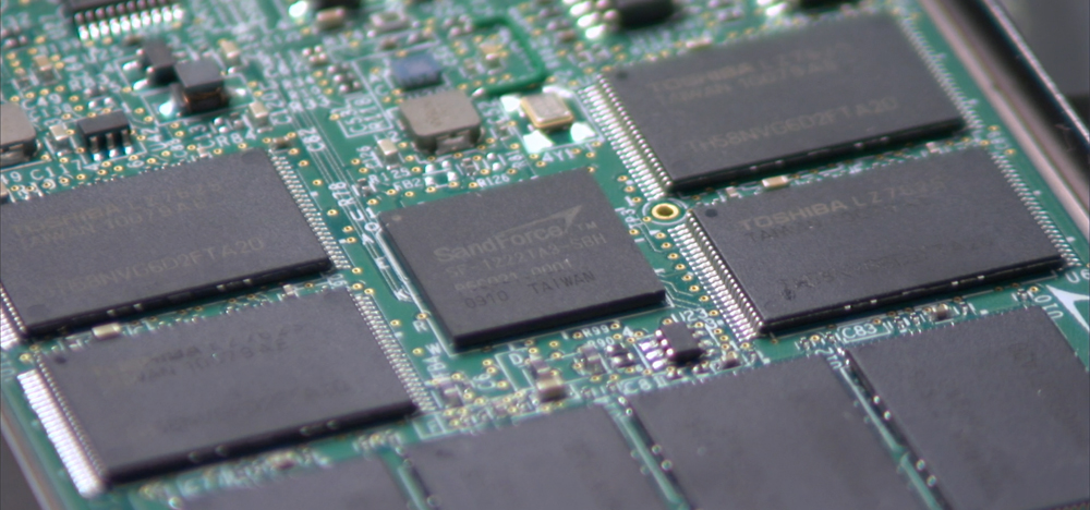 LSI's SandForce Flash Storage Processor. SandForce was acquired by LSI in January, 2012.
SSD Phases: Development
Kingston told us that they often begin prototyping within 60 days of their preliminary design, making for more efficient development and reliability engineering/testing. Development itself is one of the most involved functions of the entire process, and due to logistical limitations with prototyping, firmware programmers and engineers have had to come up with methods to simulate hardware-firmware interactions without the presence of the physical device. Here's a look at what the development phase breaks down to:
- Preliminary Hardware Design: The engineering team analyzes the documents produced in the Design Phase and focuses on what needs to exist on a hardware-level to make those requirement specifications become reality.
- Team Analysis & Review: The team runs through the new hardware design docs, block diagrams, specifications, and all documentation produced so far, then moves on to the deeper stuff.
- Detailed Hardware Design: Next the team assesses NAND Flash availability and cost structures to determine the right mix of components for the target market. NAND Flash is by far the most costly part of the BOM (bill of materials) on an SSD, so a lot of analysis is done selecting the right memory chips for the device. The team also looks at form-factor requirements as system drive bay configurations continue to shrink. Drive form-factor has an affect on the components that are used and PCB layout requirements.
- Firmware Simulation: In effort to reduce engineering downtime, while the SSD prototypes are being laid-out and developed, firmware programmers get the jump on their own work: Using FPGA devices (field-programmable gate arrays), the developers can test logic design and hardware interactions through simulation. They can then transfer their work to the actual hardware once it is available. On FPGA testing, Kent Smith of LSI told us, "When you get that chip back, there's still a whole lot of work you do inside the firmware. Half of the development is before you get the silicon, the other half is after you get the silicon."
- Tape-Out: Once the firmware prototype is ready, it's taped-out and sent to the factory for use in the SSD prototype. Smith of LSI explained this process to us succinctly:
Tape-out is a very, very old term that dates back to when you actually had reel-to-reel tapes. You would take your tape off your mainframe and send it to your manufacturer -- and it had all the code to produce the varied silicon layers (or masks) that the manufacturer would lay-out for the chip. Some chips have upwards of 10 or 15 layers, more complex chips like CPUs can certainly get into the 20s and 30s. As the number of layers increases, the cost to produce that chip increases with it.
- FW Programming on Prototype: Once the first prototypes are ready for testing, the firmware engineers will continue iterating their code to accommodate all the features and take care of as many bugs as possible. This phase bleeds into the SSD Testing Phase, covered next.
So then, the development phase is where all the details are hammered out: That's where your SSD comes to fruition, gets programmed, feature-packed, and detailed. As Crandall said, the controller is really "where the magic happens," so that means a lot of the features you enjoy in an SSD are a result of complex firmware/controller programming; this all goes into informing the hardware how to deal with read/write requests, garbage collection, overprovisioning, and other solid-state features.
When we asked Smith about the time requirements for the controller's development phase, he told us:
"Totally dependent upon the requirements. There are many more factors than what we'd desire -- some factors include Flash availability, other times you're going for a particular market timing, sometimes you need to align with a motherboard chipset. For example, when SATA III first came out, there weren't a lot of products that could talk from the host side, so a lot of devices were waiting for a chip to talk to. Sometimes you have to wait for other parts of the industry to see if you're going to be compatible."
Later in the conversation, Smith added that the overall average/predictable cycle for controller development is -- when iterating upon existing controllers (i.e. not making an entirely new product) -- somewhere in the range of 9 months to a year. However, he was keen to add that this is, again, highly-volatile and based upon several factors in the current market and technology environments.
The only thing standing between development and release is, well, more development -- testing, refinement, and fabrication follow.
SSD Phases: Testing & Validation
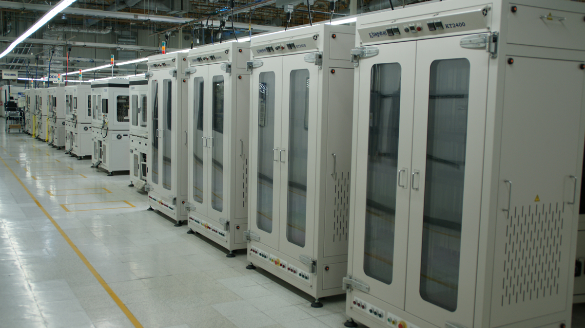 Kingston's test machines: In the foreground, we see server memory test ovens (thermal testing); the background is for compatibility testing.
Having come out of test engineering myself, I'm a bit biased when I say that test is one of the more fun aspects of hardware lifecycles. The reasoning is quite simple: My job was to break things without the requirement to fix them (issues were sent to developers and ranked by severity). Testing and validation methodologies will vary on a company-by-company basis, but the core principles are the same:
- Methodology: Test Engineers and Product Managers (the titles are variable) develop use case scenarios -- defining the likely utilizations of the device, then rank them by how likely they are to occur in the field. More common uses (like everyday uses) will be tested most heavily, while obscure ones will often be explored only if a customer requires the feature/use case.
- Procedure: After use-case scenarios are developed, test cases get written (often by non-testing engineers, so as to eliminate bias from testers and developers) to reflect these use cases. Test cases are laid-out in a step-by-step manner to guide the technician through what would (theoretically) occur in the field. Many companies have adopted automated testing, the complexity of which will vary based upon the task that must be accomplished: Where I worked, XML scripts were used to initiate tens of thousands of S3/S4 power cycles, then log the results to files. Both LSI's Flash Components Division and Kingston mentioned that they heavily utilize automated testing, for instance: LSI conducts nightly automated testing to test interim code revisions; the results are shared with the developers each following morning, who then begin work on resolutions. However, some elements require technicians to manually initialize or observe; when testing laptops, for instance, it was impossible for my team to automatically log LCD failures -- we needed human eyes for that.
- Quality Control: Reliability engineering is also a factor when testing products, and is often more applicable on the manufacturer's end than on the controller supplier's side. Crandall of Kingston told us that Shock & Vibe testing, age simulation, six-axis, and thermal/cold cycles are also used to abuse SSDs, hopefully provoking failures early so the team can address them before launch.
 Kingston's testing and quality control.
Many testing facilities will use large shock & vibration machines to do the hard work; the ones where I worked resembled tables with numerous semi-pistons that rapidly cycled to hammer the living hell out of laptops. We had drop rigs for testing maximum drop height, massive freezers to test for endurance (and also simulate years of age), and plenty more. It's a very cool environment to work in. The objective? Aside from having a bit of fun, it tests the endurance and strength of the device, and most importantly, simulates years of age within a small timespan. Because companies cannot actually test a product for years before launch, they must do their best to artificially provoke age-related failures in a controlled environment.
But Wait -- What about Firmware?
Firmware is tested the most heavily when dealing with SSDs and controllers, since the drive itself is fairly solid. Crandall elaborated on the actual firmware test cycle:
"It's rare that we receive a controller, build the drives, start the testing and then everything goes really smooth. We usually go through two or three firmware revisions during that process. Once we start testing, we probably have two to three weeks of testing to do -- and once we find a problem, we report that back to the controller vendor. They work on a solution and provide us with firmware, then that two to three testing cycle starts all over again. The testing process is lengthy, and every time there's a new firmware update, the test cycle starts all over again. All of the production testing is done in-house in multiple locations -- the only testing we would do outside of Kingston would be for application testing and only in some cases, where we use unbiased third-party resources to test our devices in real-world applications.
Kingston and LSI both mentioned that they target "weak links" most heavily, and try to focus on things that they suspect will break when abused. This means more stable processes that have been previously-refined will get less focus, but won't be ignored; time is valuable, and in order to get a functional product out the door, the engineers call the shots on what gets prioritized.
Almost there! SSD Phases: Solid-State Drive Production
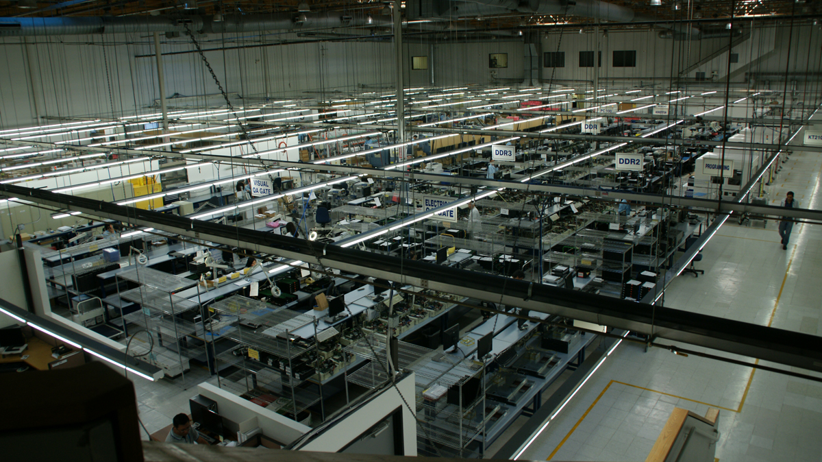
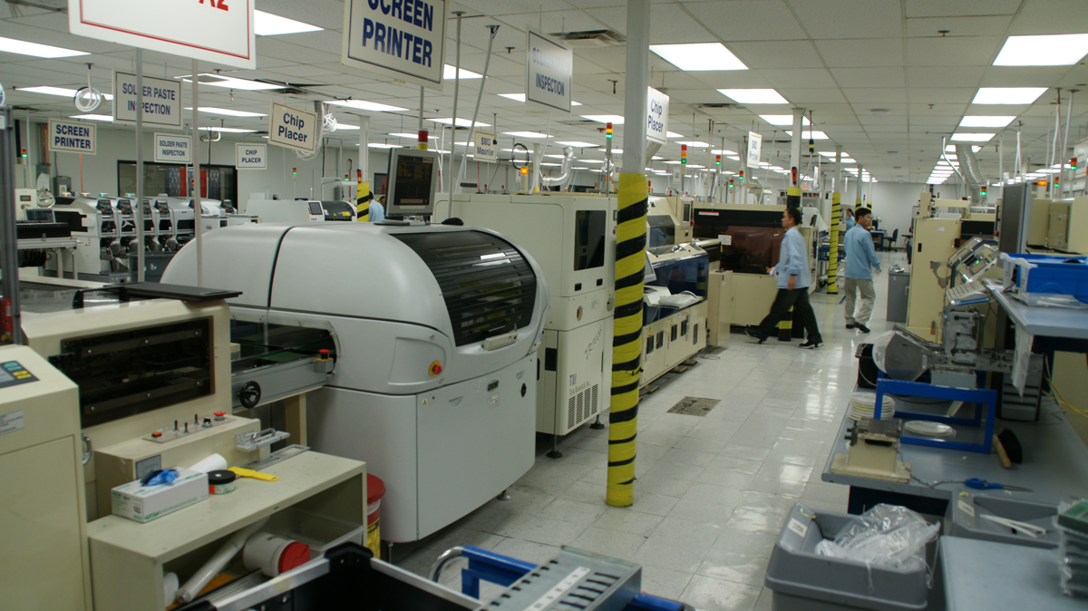 Automated SMT Lines at Kingston's Fountain Valley facility.
I've always been fascinated with fabrication and silicon manufacturing/assembly: The robotics, the to-the-nanometer precision, and the multi-billion dollar factories really make it quite easy to be truly captivated by the technology involved.
After the wafers, Flash, and other components are acquired by the factory (as ordered by the manufacturer), and after the wafers have been diced into dies, the factory sends all these parts through what are called SMT lines and reflow machines.
Kingston, as with other manufacturers, uses SMT lines (Surface-Mount Technology) to prepare the PCBs and solder chips to them all in a few automated steps. It's a very efficient system that's been in use for years now and is part of what makes mass production a possibility.
The great thing about surface-mount technology is that it's much more tangible than the previous steps we've covered, so I'll leave this video for you to enjoy before we move on:
Pretty cool, right? This is just a small example of how they work. The SMT lines themselves are fairly standard -- Kingston's, for instance, can be used for RAM or SSDs, they just need to be preconfigured for the technology they'll be processing. To illustrate the fabrication technology's flexibility, Crandall told us that Kingston uses the same SMT lines that are used by motherboard companies, and explained that it's mostly configuration and design tweaks that change the output.
Crandall illustrates the process best:
"Kingston primarily procures NAND Flash from the major NAND suppliers (Toshiba, Intel, Micron, etc.) and builds SSDs and other Flash devices with these components. We also do some of our own backend wafer processing in our facilities in the Far East. We buy wafers from major fab companies and grind, cut, package and test our own Flash chips. So it's not impossible that one day you could open up a Kingston product and see a chip with the Kingston name on it.
We design all of our PCBs in-house as well so once we have our mass production run of PCBs, they get loaded onto our SMT lines. The first step in the process is to apply solder paste in each location a component will be placed. Next, we place capacitors and resistors onto the PCB, then we have another machine that places the NAND Flash, controller and any other specialized controllers that go onto the drive. Then it goes through our reflow machine, which is something like a big oven -- that's where all the components are soldered onto the PCB. Next, it’s onto the quality control processes and finally off for testing, and then it's done."
Final Thoughts
Whenever we ask our regular readers what topics they'd like us to explore, the answer has consistently (for almost a year now) been "SSDs." That's for good reason, too; as HDDs are moved into a more archival role, we see SSDs attempting to minimize the largest bottleneck in the system: Storage. Storage devices have been historically slow, given their mechanical roots, but Flash storage is a step away from that. Solid-state storage is still growing as a technology, and as controllers and manufacturers continue "get better," to use Crandall's words, at the whole process, we'll hopefully see a widespread shift to faster primary storage.
It's pretty insane when time is applied to this entire process: Six months is what it takes on the manufacturer side (or at least, on Kingston's side), and somewhere in the ballpark of a year is what LSI might take on their next generation SandForce controller. Of course, there is some overlap during testing and constant communication between all parties, because at the end of the day, everyone in the hardware industry impacts one another. All of this design, development, firmware programming, testing, features analysis, and fabrication goes into the 2.5", speedy drive that is eventually installed in our PCs.
If you have further questions about SSDs or this article's topics, feel free to leave a comment below or on our hardware forums!
- Steve "Lelldorianx" Burke.
Additional input from GN's Hardware Editor, Patrick Stone.
Special thanks to all parties involved, as enumerated above!