The Steam Deck OLED features numerous changes to its motherboard, battery, fan orientation, and more
The Highlights
- The Steam Deck OLED’s die has seen a process shrink from 7nm to 6nm
- The Steam Deck OLED features a more barren motherboard, but that isn’t necessarily a bad thing
- The Steam Deck OLED features positive repairability changes to its controls
- Original MSRP: $550 - $650
- Release Date: November 16, 2023
Table of Contents
- AutoTOC

Intro
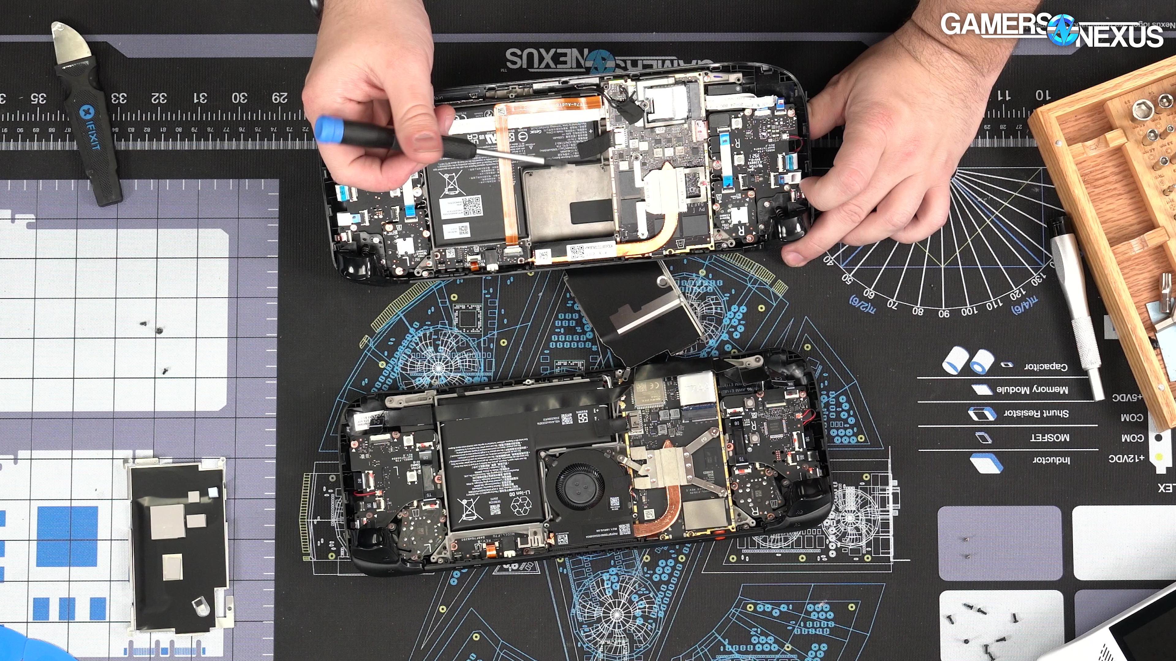
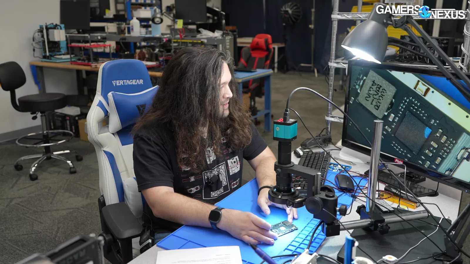
A ton has changed with Valve’s Steam Deck OLED. So much so that we got onto a call with three of Valve’s engineers and talked about changes to the power topology of the motherboard, the consolidation of two sets of daughter boards for controls, and about the changes to the heat sink and thermal solution. Valve also ended up flipping one of the Steam Deck OLED’s fans upside down from its original orientation, marking a major change to thermal design.
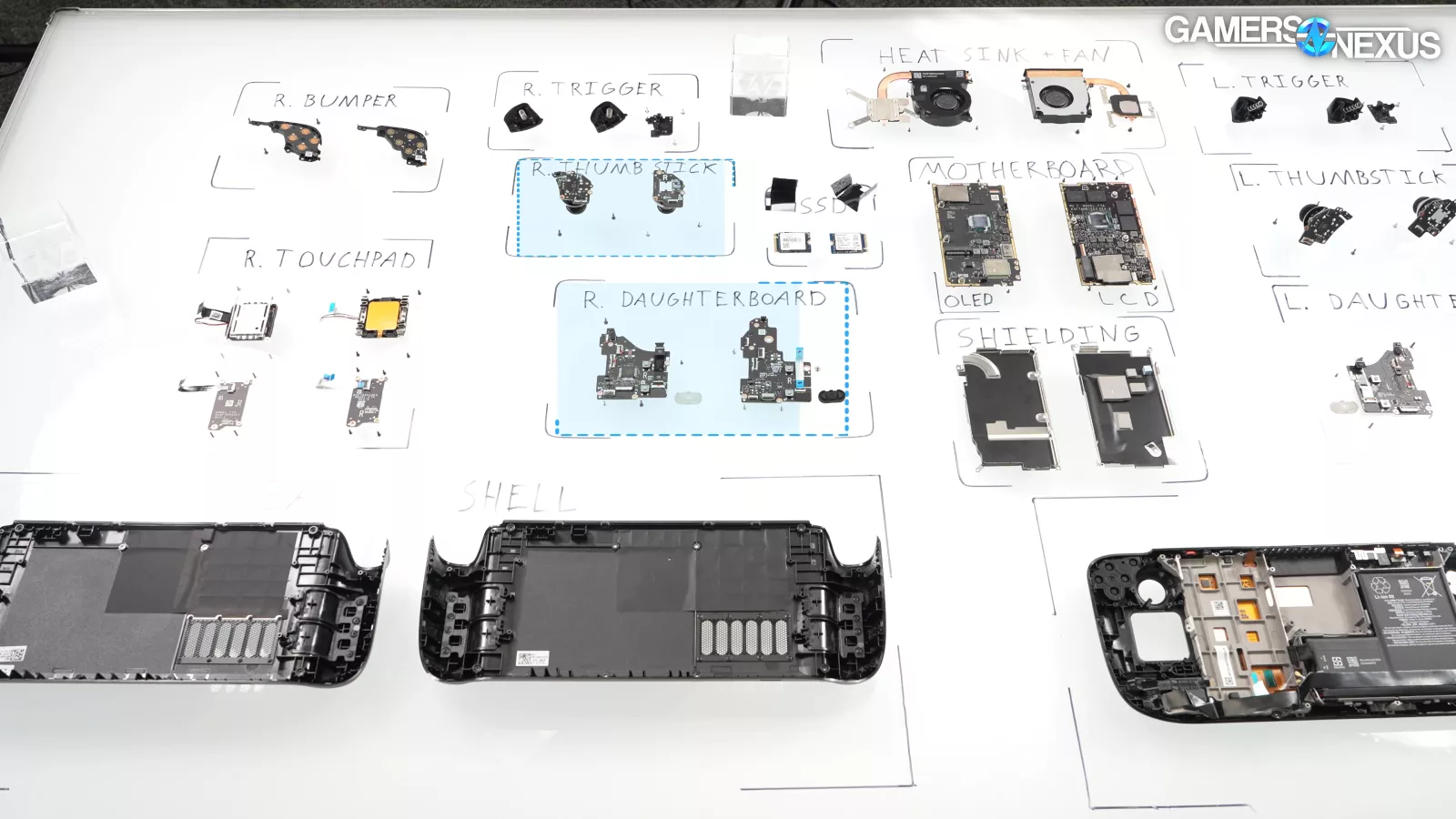
The Steam Deck OLED is almost a completely new device, and we’re going to go in-depth to talk about what’s changed in this tear down.
There’s a lot to go over, so let’s get started.
Credits
Host, Writing, Tear-down, Editing
Steve Burke
Tear-Down
Jeremy Clayton
Camera, Video Editing
Vitalii mAkhnovets
Video Editing
Michael Gaglione
Writing, Web Editing
Jimmy Thang
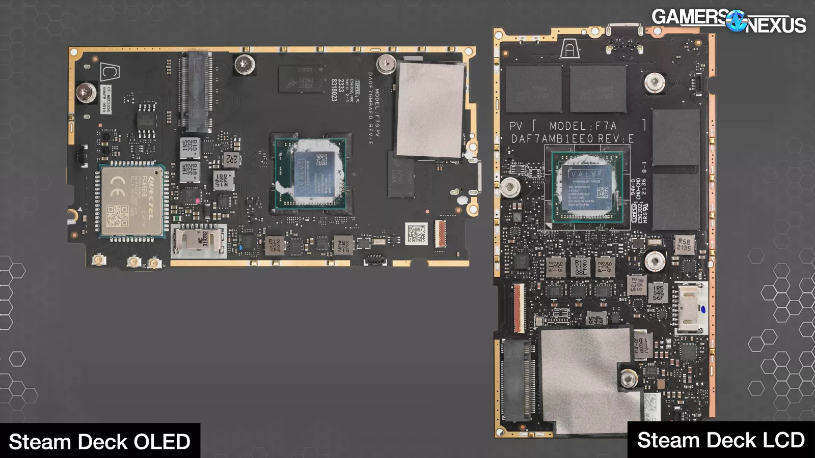
Steam Deck OLED vs. LCD Differences
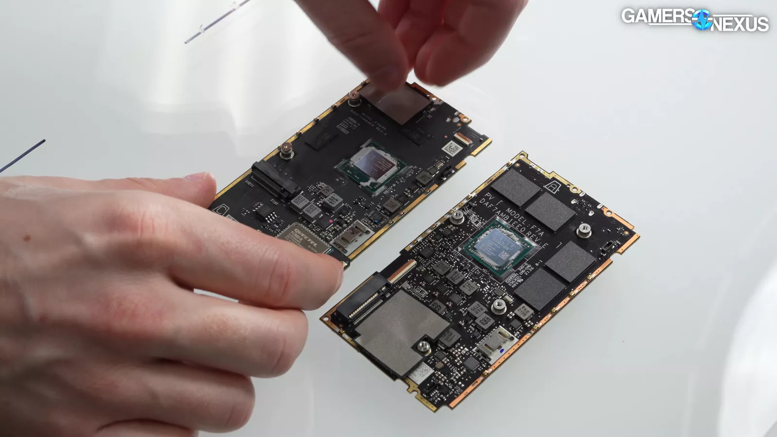
We’ll start with the die and motherboard differences. Comparing the Steam Deck OLED and LCD to each other requires a full review with benchmarks (which is on the way), but even just the physical hardware changes are significant. These include differences in not only the obvious (the screen and bettery), but also memory and silicon differences. Efficiency can be a benefit here.
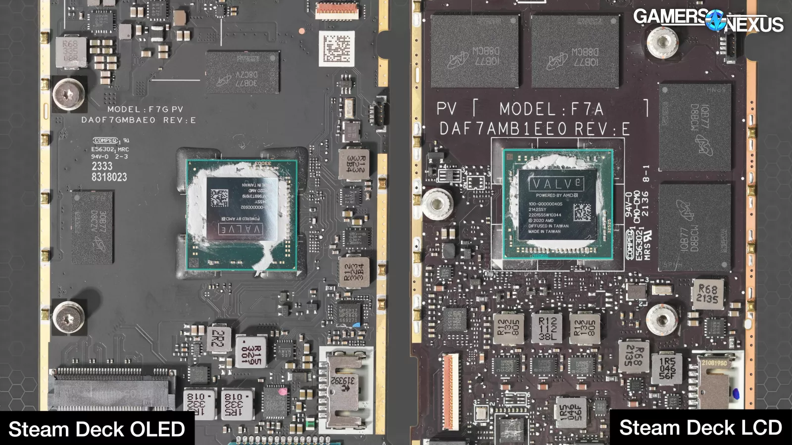
OLED vs. LCD Deck Die
The die is the most significant: Despite being the same spec, the node shrink to 6nm from 7nm brought with it a die shrink. We also noticed that Valve rotated the die, which you can see by looking at the tiny indicator arrow at the corner of the silicon substrate. This rotation has a big impact on board layout, as it changes the side the memory and VRM need to be on.
For a truer like-for-like comparison, the images actually should look more like the above. We’ll come back to this later.
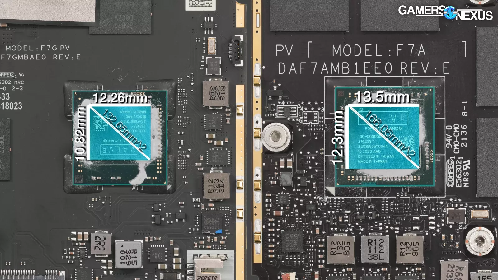
Using a barbaric and hamfisted measurement method of calipers around the structural bulk silicon of the die, but in a like-for-like measurement, we found that the new die is about 12.26 x 10.82mm, or 132.65mm^2. The old die with this method was a much larger 166.05mm^2, or about 13.5 x 12.3. For reference, the official measurement on this is 163mm^2, so we’re only off by a little bit considering we’re counting bulk silicon and doing a hand measurement.
Steam Deck OLED Motherboard Differences
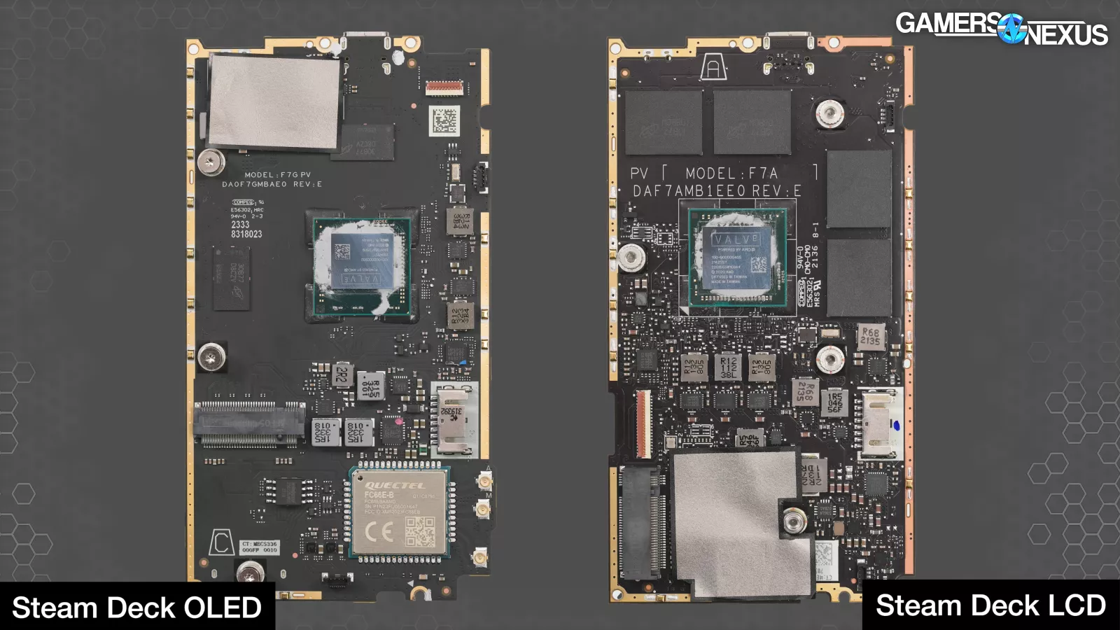
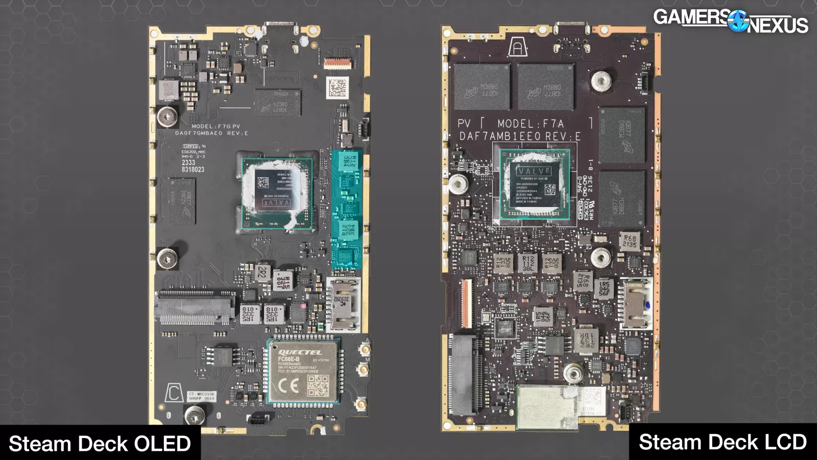
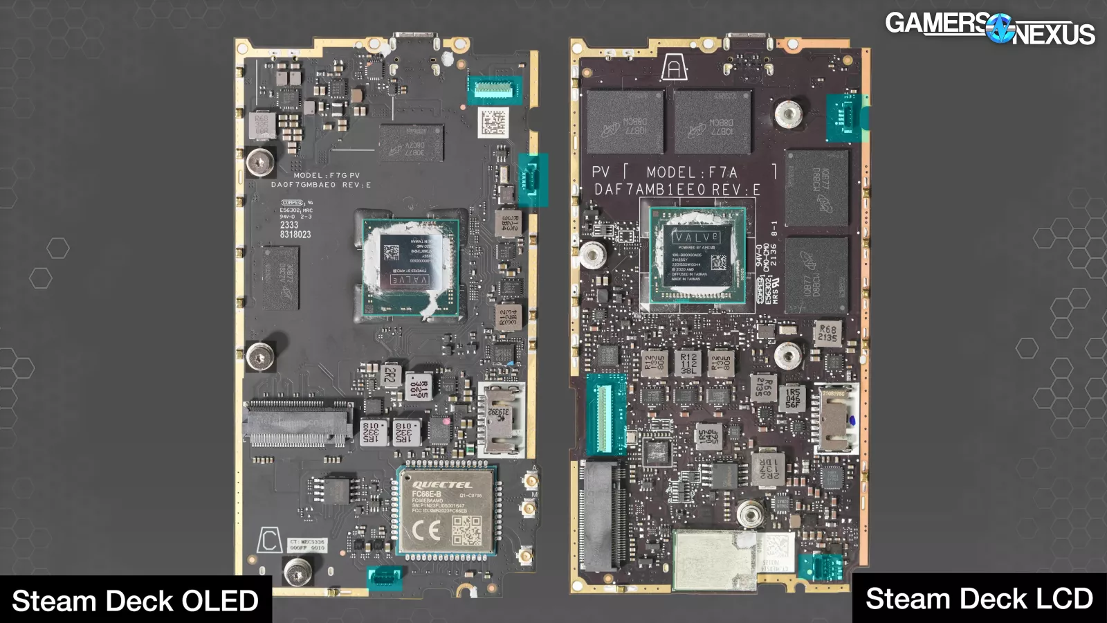
Looking at the rest of the motherboard, there are small differences everywhere. Some of these are from the refreshed Deck Valve did previously, but we’ll cover all of the differences from baseline.
First, Valve has significantly cut down on the density of components (and even just bare solder pads) with the new board. The board is more barren. That’s not necessarily a bad thing, but it probably helps with cost too.
Talking with Valve, this reduction of component clutter is an optimization: The board was overbuilt previously as Valve wasn’t sure where the Steam Deck would end up next, but now that they’ve refined it, they can reduce the components that a pick-and-place machine end up planting all over the board. Valve says cost was not a factor as the parts are extremely cheap, but it was more about optimizing the layout and efficiency of the design.
Steam Deck OLED vs. LCD Memory (RAM/VRAM) Changes
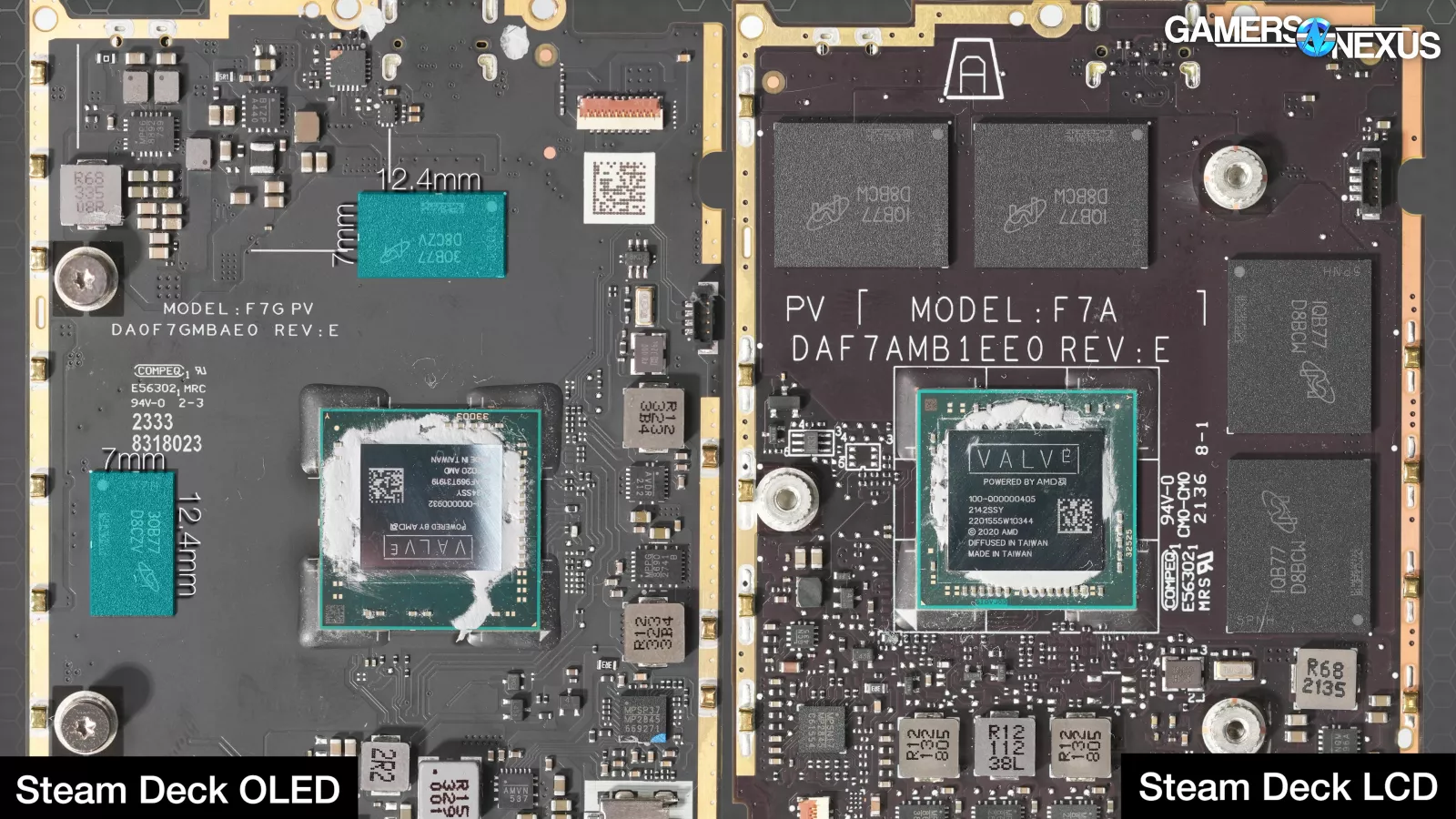
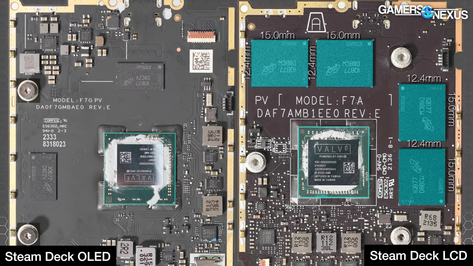
The biggest change is to the memory: Our old unit used 4 of Micron’s 32Gb D8BCW modules, which are the larger 12.4x15x1mm modules. These took a huge amount of board space on the old Deck and forced other components into more compacted areas elsewhere on the board. The new Deck OLED moved to significantly smaller 12.4x7x0.5mm modules and only uses two of them, because they’re 64Gb density to achieve the same 16GB capacity. Making this change saved Valve almost 570mm^2 of area, which is huge.
That space isn’t just unoccupied. Although the memory traces aren’t visible on the top layer of the PCB, Valve utilized the layers within this large empty space to route memory traces. A lot of memory traces need length-matching where the traces have to be the exact same length for performance reasons. Valve used this space to run traces and get the correct length for each run. Valve said that it took two months alone just for the memory layout -- and we know from motherboard manufacturers that memory topology can be a make-or-break part of the design process.
This is made harder by the fact that Valve is using higher-quality, denser memory modules. Each individual module has more traces than when Valve relied on the 4 DIMM packages previously.
Deck OLED vs. LCD VRM & Power Delivery
The VRM is next. The APU VRM is mostly the same spec, but Valve has increased the rail count board-wide and improved power delivery elsewhere.
The biggest change for the APU phases is the location: The original board had the power delivery centrally, moving the power delivery components south of the APU.
The new board shifted some of the power stages to the right of the APU, occupying space where the memory used to be. But this is also because the die physically rotated, which shuffled the memory modules correspondingly.
The new inductors are also higher efficiency, taller inductors in some cases that are easier to sink the heat to the cooling solution.
This is for thermal reasons. MOSFETs and particularly inductors are high heat-generating components and will increase heat of everything surrounding them. Previously, these were located centrally on the PCB and heated everything else up.
Now, they’ve moved them closer to the fan -- which is intended to help with cooling -- and they’ve also gotten the large 1mm tall memory modules out of the way. The VRM has more access to air and the heat gets more evenly distributed.
The new memory is also a new process node and more power efficient, so it is less in need of direct cooling than the VRM. Memory is a relatively low heat flux component.
We asked about the absence of some of the filtering capacitors around the APU, where previously there was just a lot more density of surface mount devices. Now in theory, the engineering answer for this from Valve’s engineering team was that the reduction in impedance or cross talk between the VRM and the APU drives down the need for quite as many filtering capacitors in general to stabilize the APU.
Deck OLED WiFi, BT, & Cables
There were also a number of cabling changes on the board. These aren’t significant, but we’ll highlight some headers that have moved around. This is just to accommodate the new board layout.
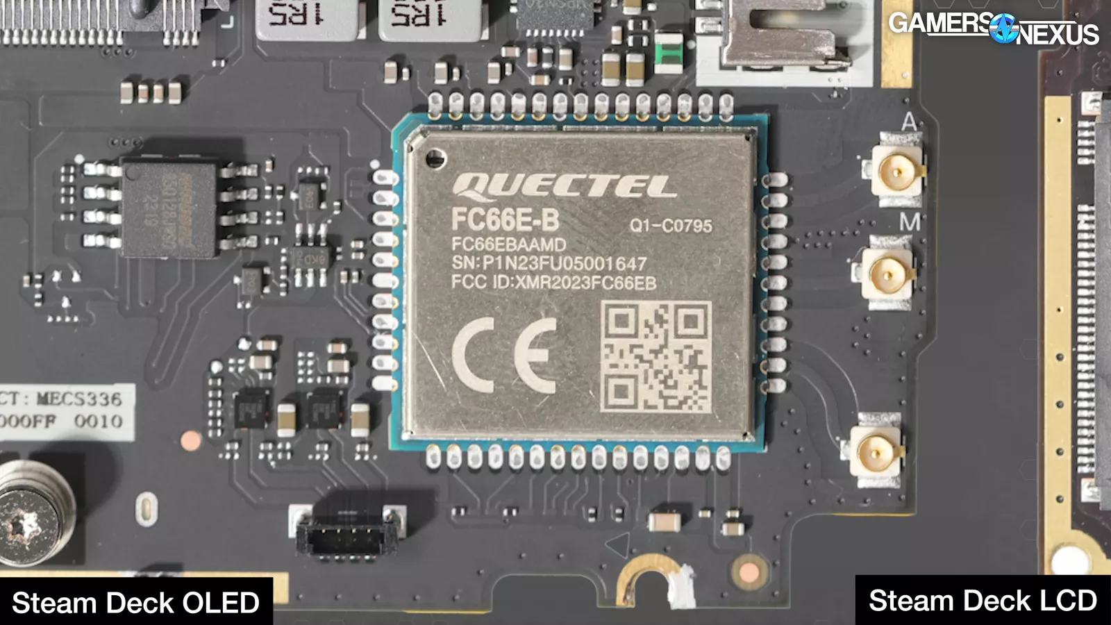
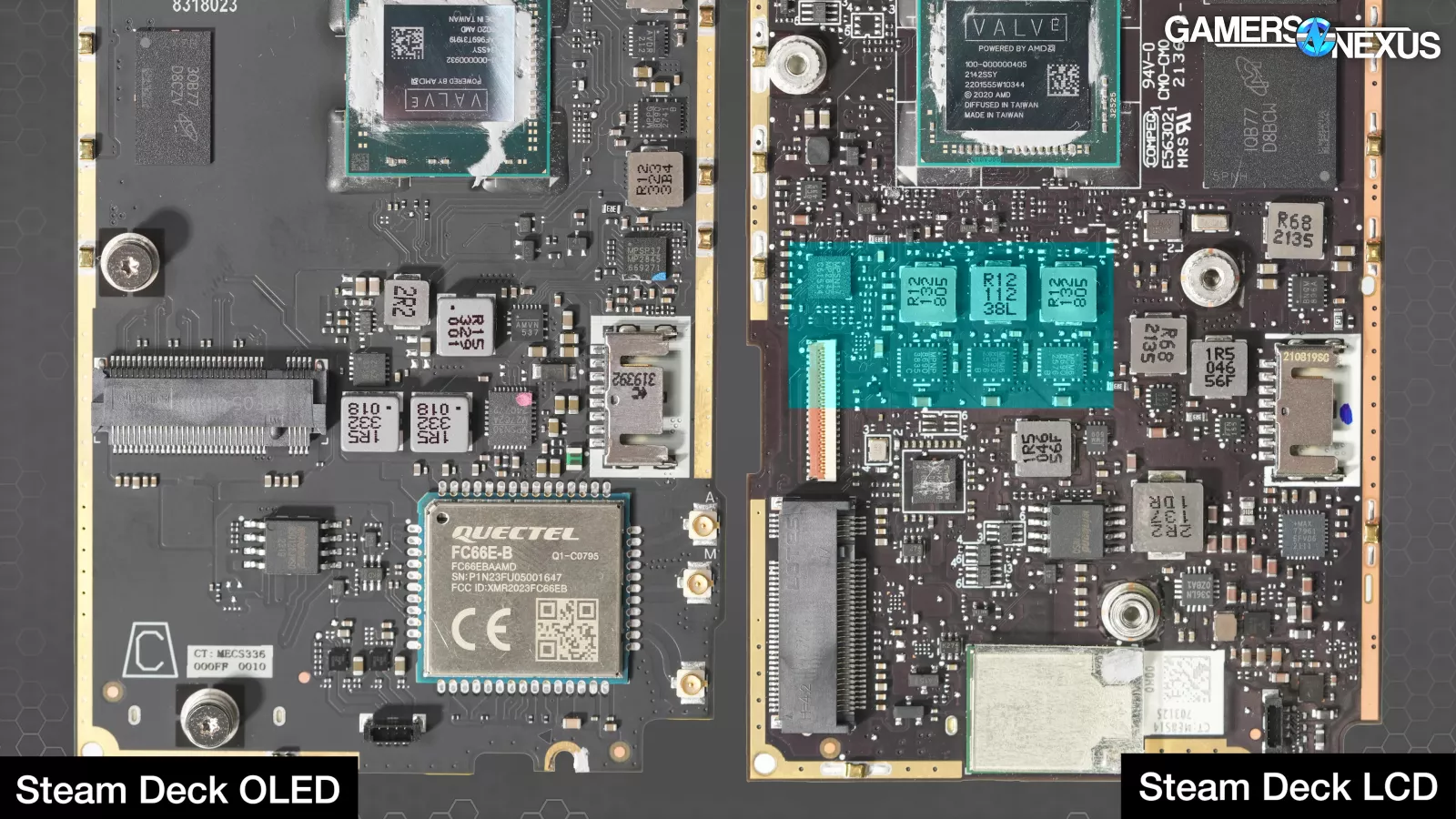
The networking has changed completely with the Steam Deck OLED. The OLED moved to WiFi 6E and uses a Quectel FC66E-B module with a max data rate of 3000Mbps and maximum temperature of 75 degrees Celsius.
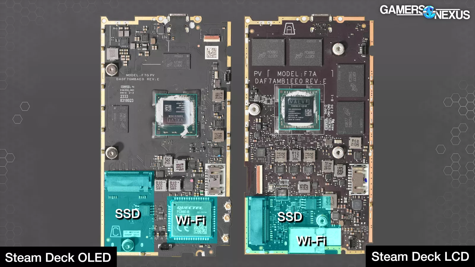
This module is moved to the right of the SSD, whereas the older LCD model positioned its networking hardware underneath the SSD and with some shielding on top.
Disassembly: Power Circuit, Charging IC, & Cooling
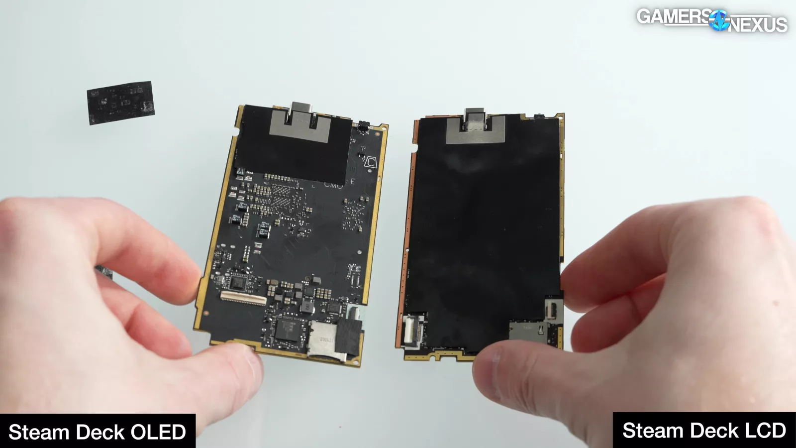
Finally, the back of the motherboard is fully covered and populated on the old unit and uses some tape to cover this up, while the newer board is more barren -- matching the top-side -- and simplified. This is an efficiency change.
Steam Deck OLED Cooling
The cooling solution has also changed a lot, and some of the changes jumped-out at us right away.
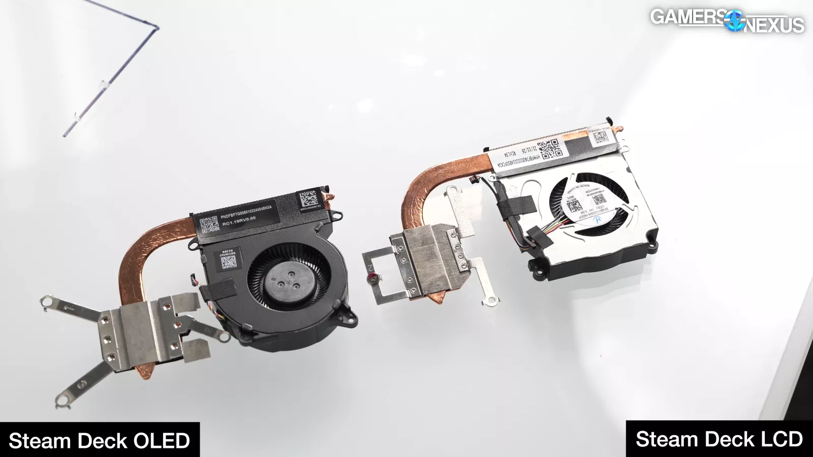
First of all, they flipped the fan over. Previously, the blower fan was positioned to move more air across the shieldcan of the Deck.
Valve has significantly changed the shield can and no longer sinks heat into it as directly, eliminating the thermal pads. This is still usable surface area, but efficiency improvements may have reduced the need for it.
Flipping the fan allows it to force more air through the actual finstack at the cost of reduced airflow through the shield can and motherboard area. This should lead to more efficient heat exchange in the heatsink, or faster dissipation.
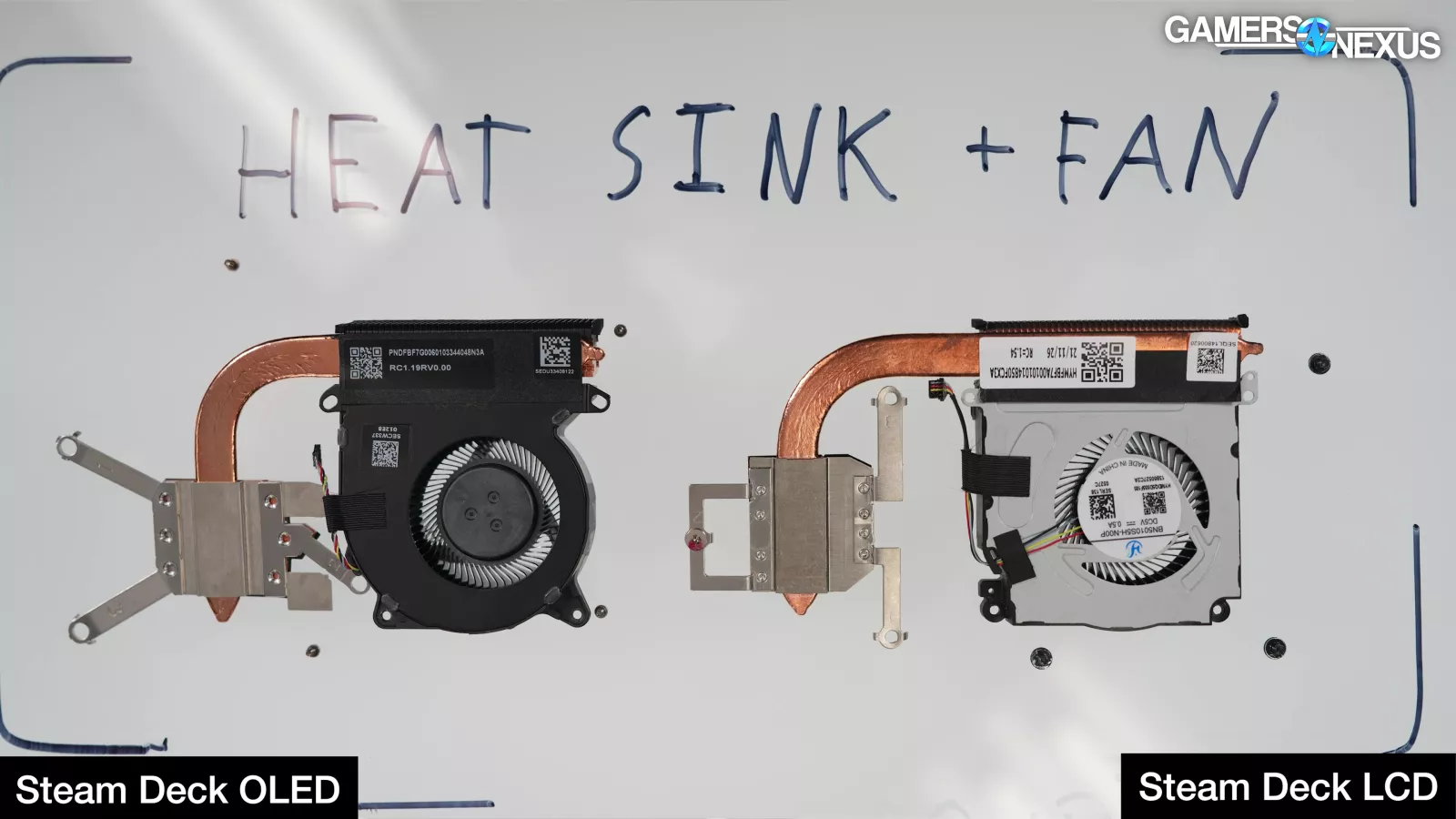
Valve’s changes also included increasing blade and impeller thickness, along with a thicker finstack altogether. The thicker finstack was possible due to the reduced screen thickness caused by moving to the OLED display. The fan changes should promote more flow at similar pressure, while the larger finstack just provides more surface area.
We also expect to see a big impact to the frequency profile of the Deck in our hemi-anechoic chamber testing, which we’ve begun running tests on that you’ll see in our upcoming review of the Steam Deck OLED.
Changes to the blade thickness and fan thickness will impact the spectrograph. Valve had some higher whines in its original design, depending on which fan you got. Valve told us that its 2-4KHz tones should be reduced. We’ll validate that in testing soon in this chamber.
Steam Deck OLED Charging Circuit
We also noticed that the charging circuit is significantly different. This is something we tested in our original review and found to be the hottest component on the board, sometimes entering the 90s C when charging and gaming, like when docked. It was also the only component where we were specifically worried about longevity.
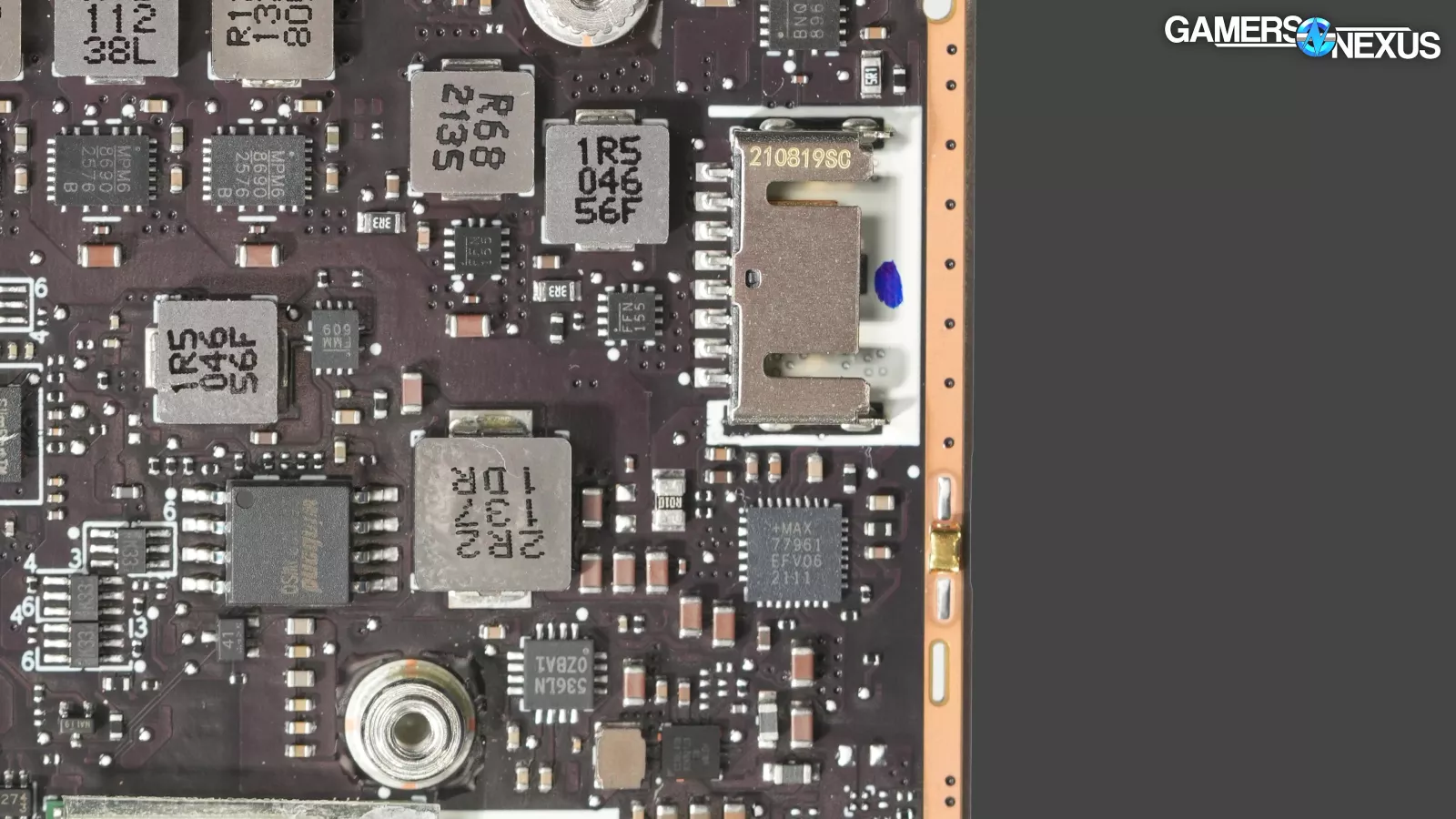
The original charger IC was located right below the battery cable on the motherboard, and from looking around, it does appear that some people had these scorched.
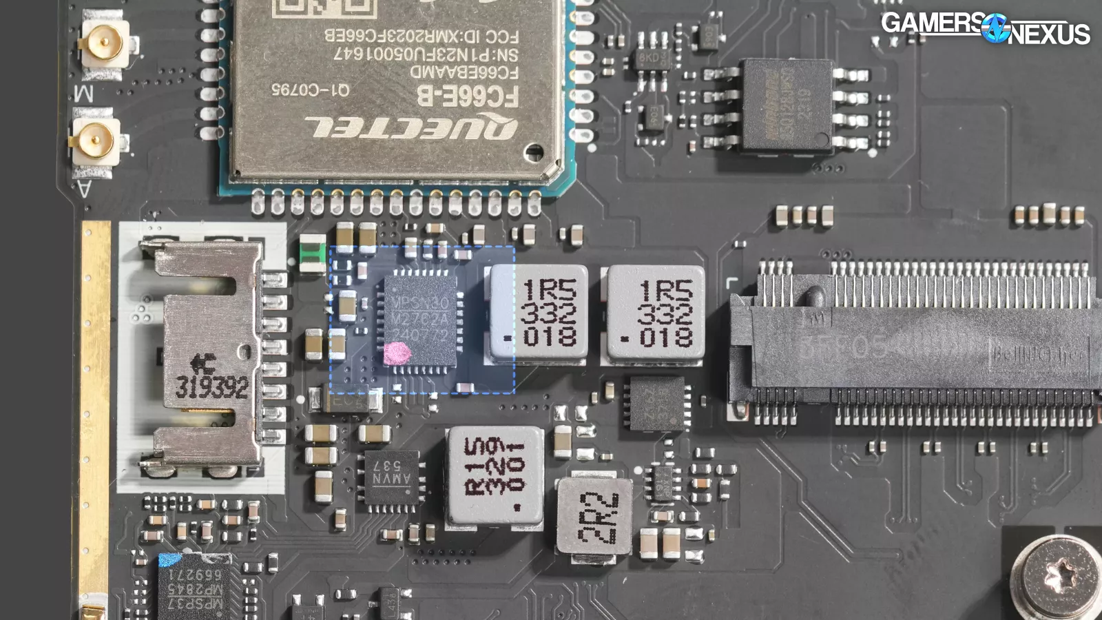
The new IC is labeled as an M2762A unit, which maps to the Monolithic Power Solutions MP2762A dual-phase interleaving buck charger. Assuming Valve used this exact model without changes and we found the right data sheet, the sheet is dense with functional schematics and charts explaining its operation as a dual-phase charger IC.
This IC is a pretty big difference that we weren’t familiar with before looking into it a bit more. Valve explained this solution as using duplicate MOSFETs and inductors to spread the power and heat load over a wider physical area. Valve said it could be thought of as running two charger ICs in parallel. The heat is less concentrated, making the IC more efficient due to reduced heat at the onset.
This new solution should distribute heat better.
Although ICs like this can be reconfigured in some cases, the default “absolute maximum ratings” table indicates a 150C junction temperature max, with an earlier section of the document indicating safeties at 120C.
Valve also made a number of other changes across the platform that are harder to see. They’ve reworked the power topology to add more rails and have changed some miscellaneous regulators.
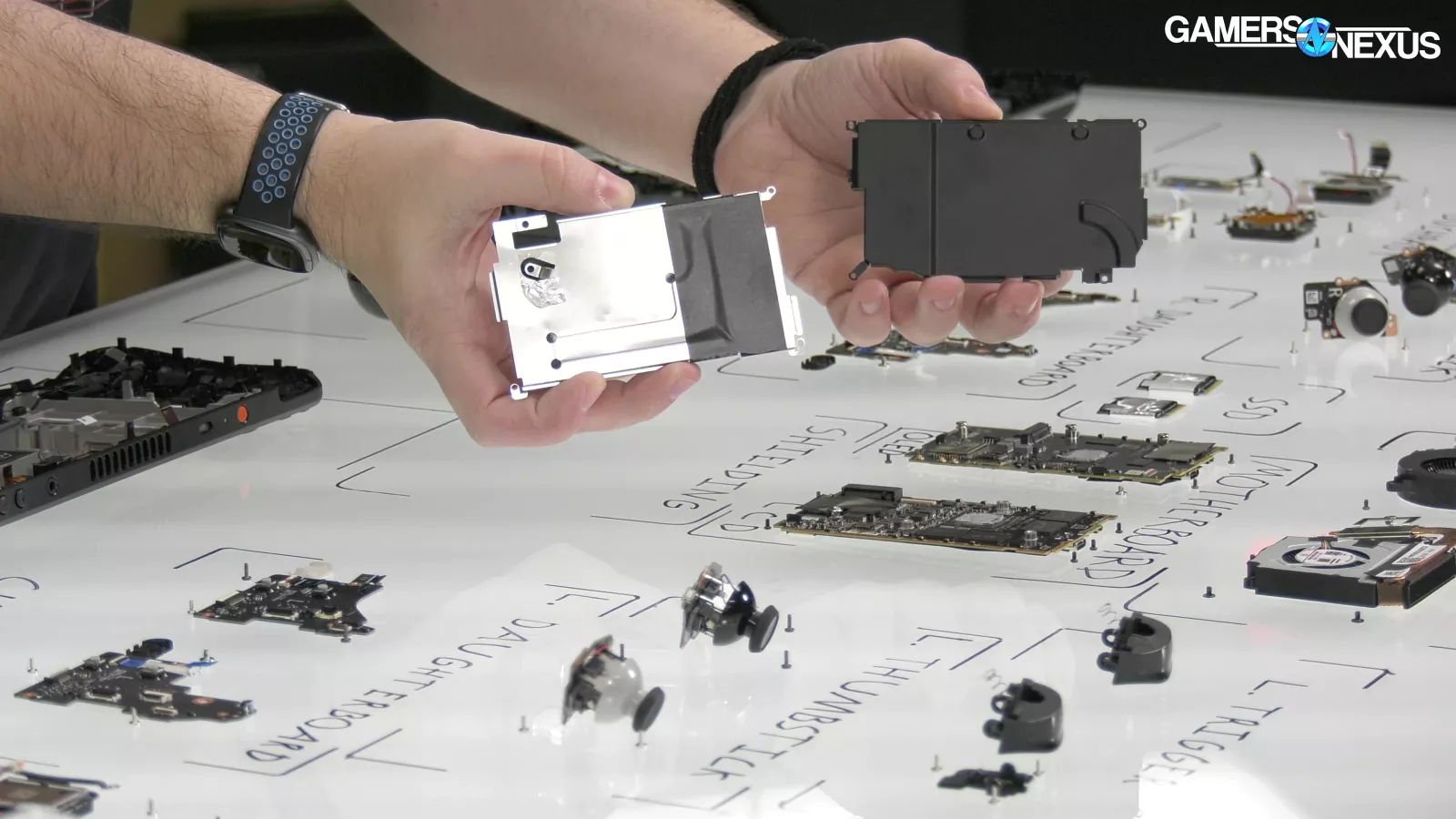
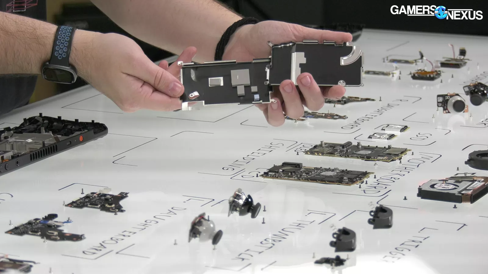
Steam Deck OLED Controls
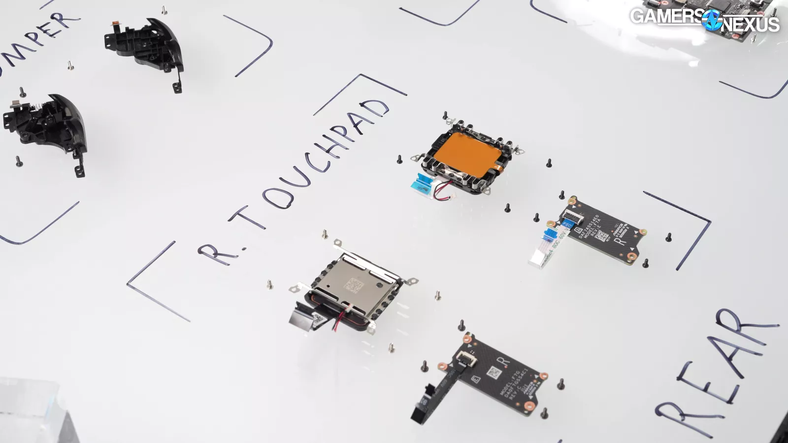
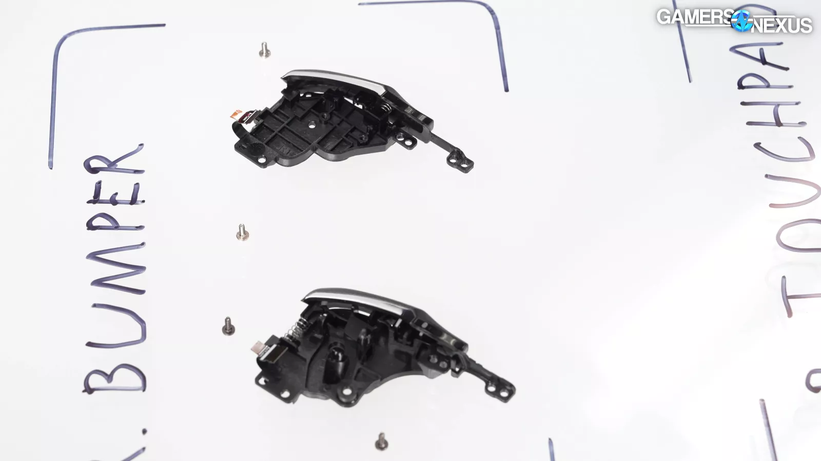
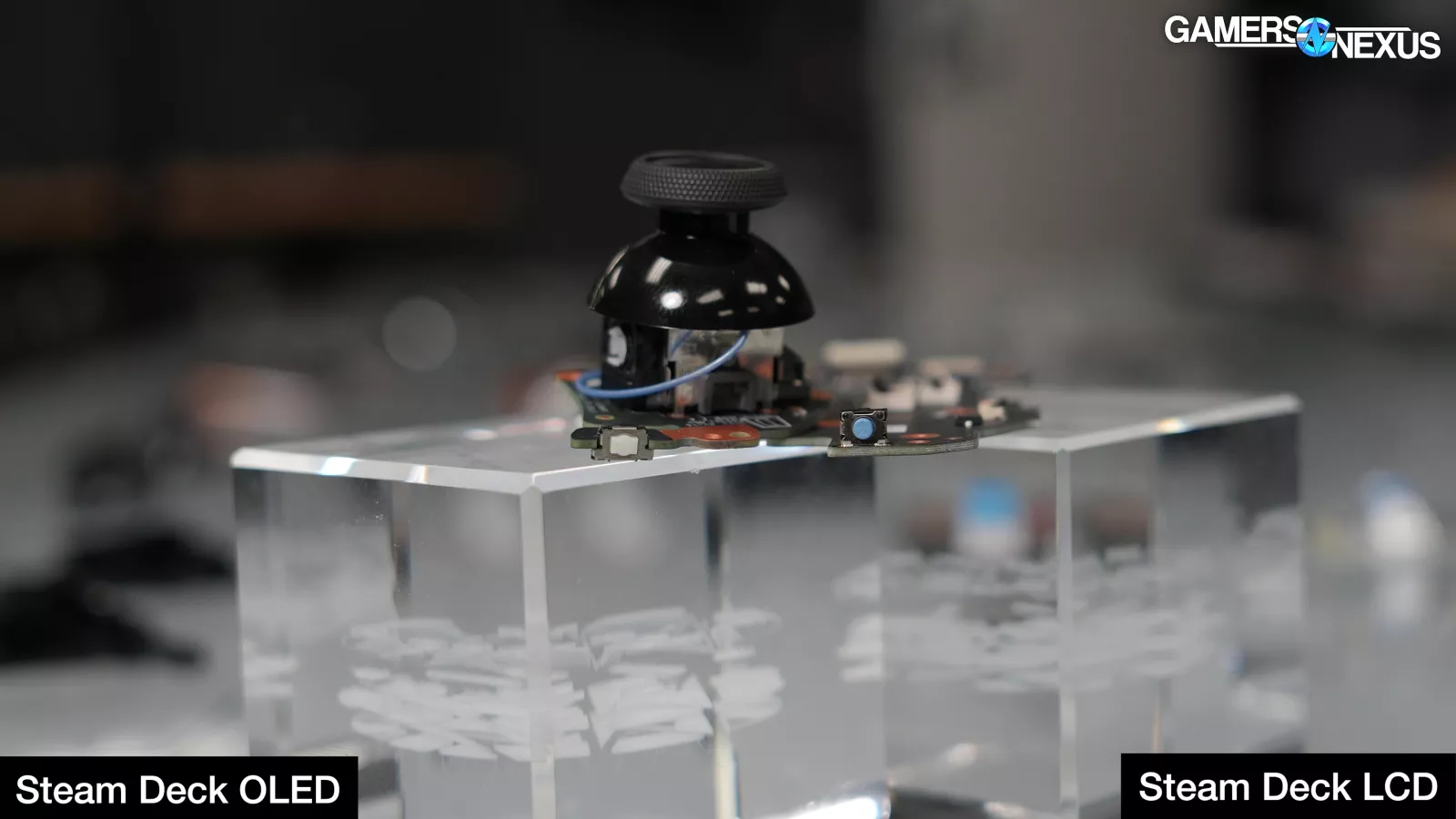
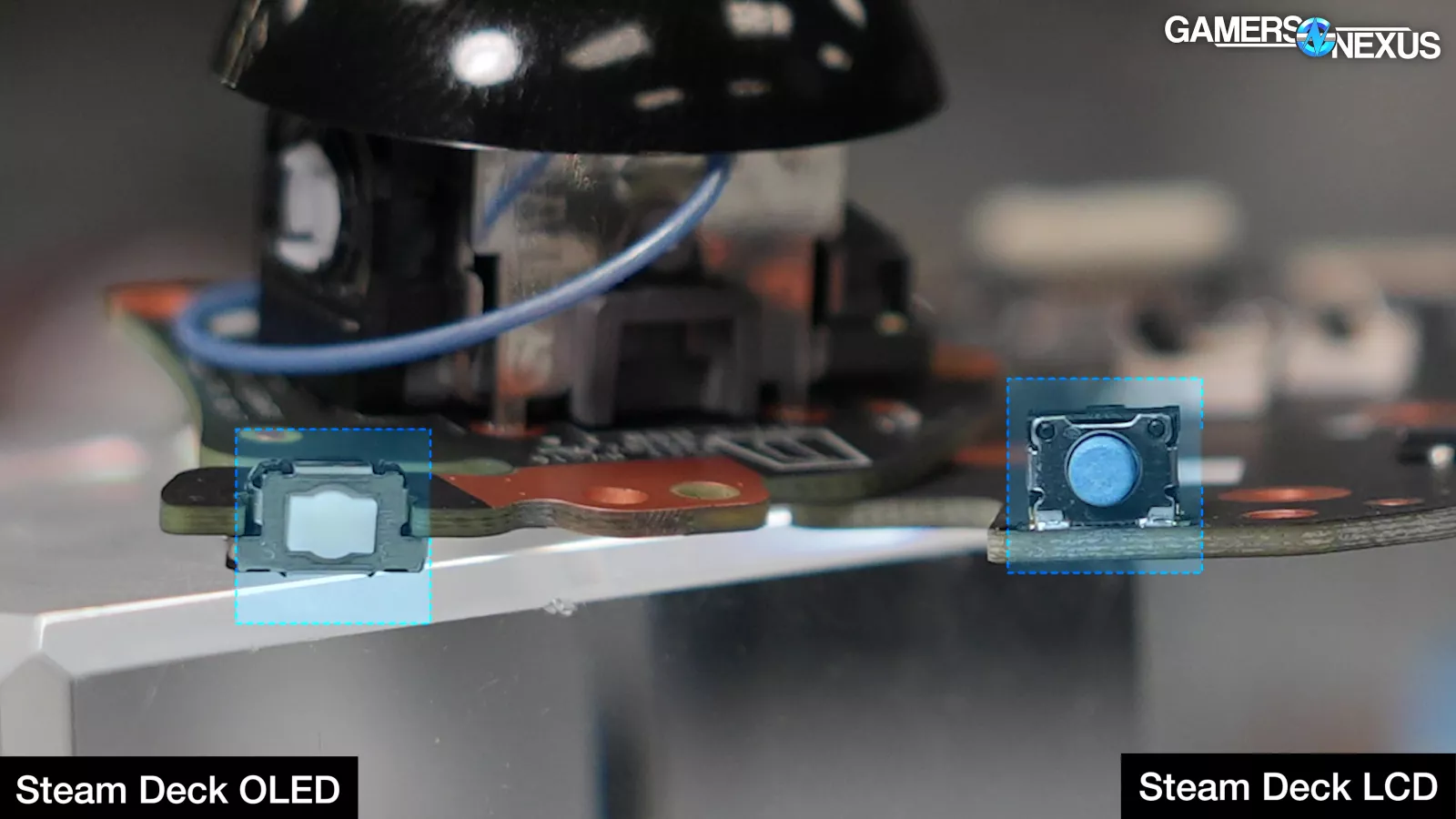
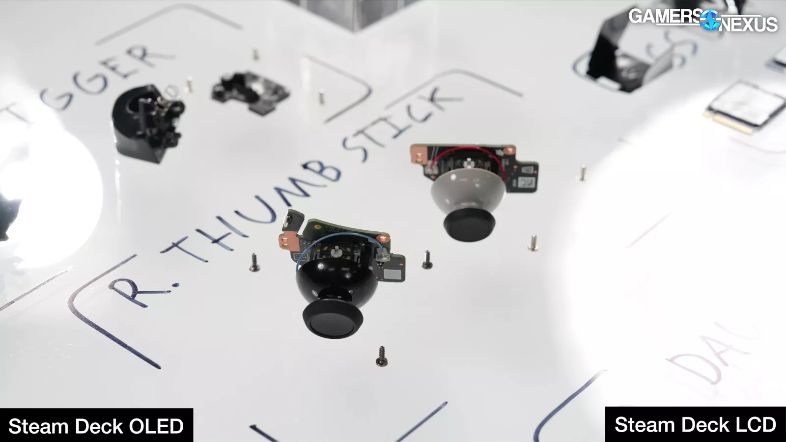
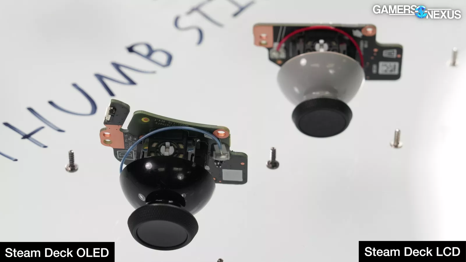
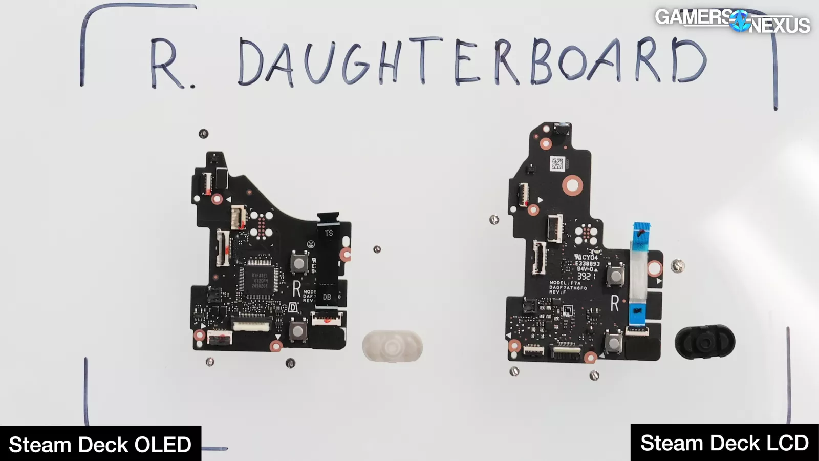
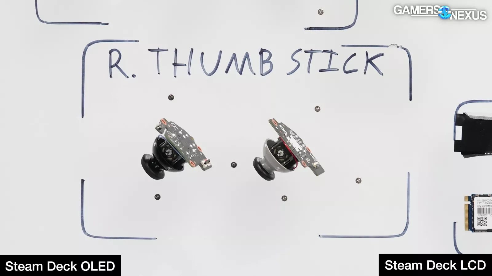
Our final section gets into controls, where Valve had some relatively large changes. The first thing we noticed was the change to the analog stick and bumper button. Valve moved the switch for the bumper off of the larger daughterboard and instead onto the PCB containing the analog stick itself.
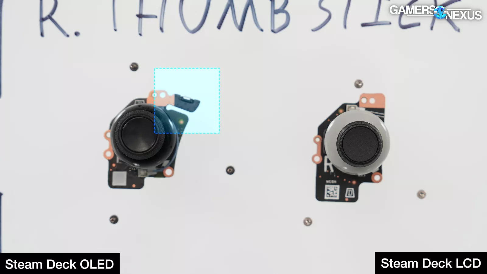
The switch has been changed, with Valve now using a higher endurance switch instead. This is in addition to reworking the stick PCB to jut out with a peninsula to meet the bumper button. Our only concern with this was that it may create a weak point. Valve claims that some flex is part of the design and that they are using redundant traces, which should provide better survivability in falls even if there’s a micro fracture somewhere. The peninsula is part of the shock absorption. Without doing drop testing on a high sample size of devices, it’d be hard for us to prove or disprove this.
Other than improving resistance to fall damage, the change also makes things simpler to repair and maintain as fewer parts will need to be removed to make a repair of this region of the device.
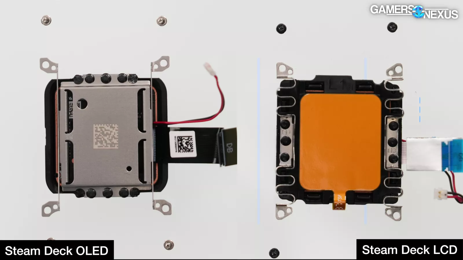
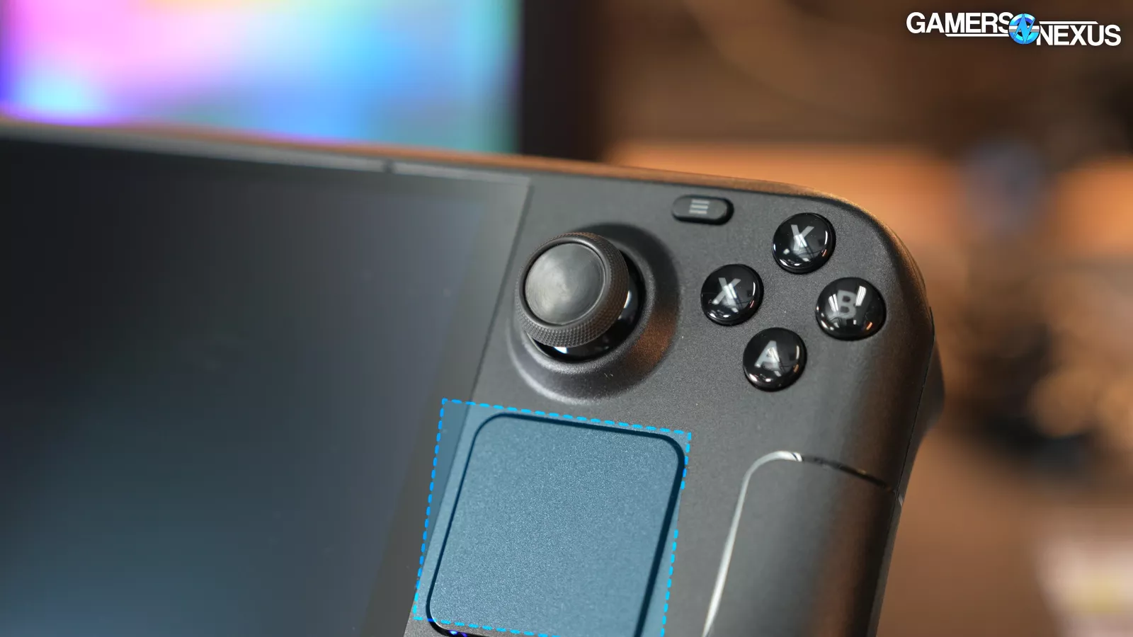
Valve also significantly changed its touch input module: We noticed that it used to have a squiggly metal retention spring as part of the touchpad mounting. Now, the spring is straightened. The trackpad module now has fewer overall parts, which other than an efficiency improvement, should also reduce points of failure by improving tolerances. The touchpad also feels different in use, and Valve stated that it “expects trackpad repairs to go down to near 0.”
We found that it is now easier to remove the trackpad module due to better clearances with the chassis.
Steam Deck OLED Chassis
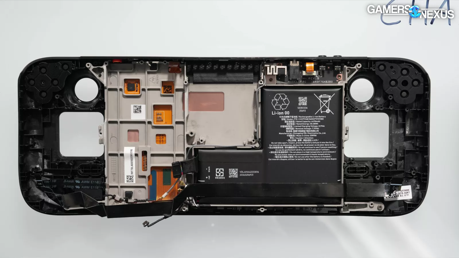
The screen itself allowed most of the physically constrained changes. For example, by moving from LCD to OLED, the battery is now thicker as a result, which means going up from 40 watt-hours to a 50-watt hour solution. The new panel also changed the mounting in the frame. The magnesium subframe for the device now has the OLED cable routed on the opposite side, which makes it easier to replace the screen. We haven’t yet tried to remove the screen as we still need to complete other testing, but it is supposed to be removable without disassembling the device to this level -- which would be a big improvement.
Steam Deck OLED Tear-Down Conclusion

This is about as detailed of a tear-down we could pull off within 24 hours. Opening the Steam Deck OLED up, it’s clear that Valve has changed a lot of things. It’s clear that this is not just a screen refresh. The motherboard, for instance, also changed in significant ways, especially on the charging side of things. These changes should be beneficial as they distribute the heat load across the board more evenly. The cooling solution is also very different and we suspect there’s going to be a big change in frequency response, which we’ll test in our hemi-anechoic chamber.
The control reworks were also somewhat unexpected for something that’s “just a screen refresh,” which seem like positive changes in the name of repairability and maintenance. This is awesome to see from Valve.
We still have to do our thermal, acoustic, and power testing in an upcoming review. That’s where we will be validating some of Valve’s claims and looking at how much the company’s changes really affected things from a function level. Make sure to check back for that.