Frequency is the most advertised spec of RAM. As anyone who’s dug a little deeper knows, memory performance depends on timings as well--and not just the primary ones. We found this out the hard way while doing comparative testing for an article on extremely high frequency memory which refused to stabilize. We shelved that article indefinitely, but due to reader interest (thanks, John), we decided to explore memory subtimings in greater depth.
This content hopes to define memory timings and demystify the primary timings, including CAS (CL), tRAS, tRP, tRAS, and tRCD. As we define primary memory timings, we’ll also demonstrate how some memory ratios work (and how they sometimes can operate out of ratio), and how much tertiary and secondary timings (like tRFC) can impact performance. Our goal is to revisit this topic with a secondary and tertiary timings deep-dive, similar to this one.
We got information and advice from several memory and motherboard manufacturers in the course of our research, and we were warned multiple times about the difficulty of tackling this subject. On the one hand, it’s easy to get lost in minutiae, and on the other it’s easy to summarize things incorrectly. As ASUS told us, “you need to take your time on this one.” This is a general introduction, to be followed by another article with more detail on secondary and tertiary timings.
What Are Memory Timings?
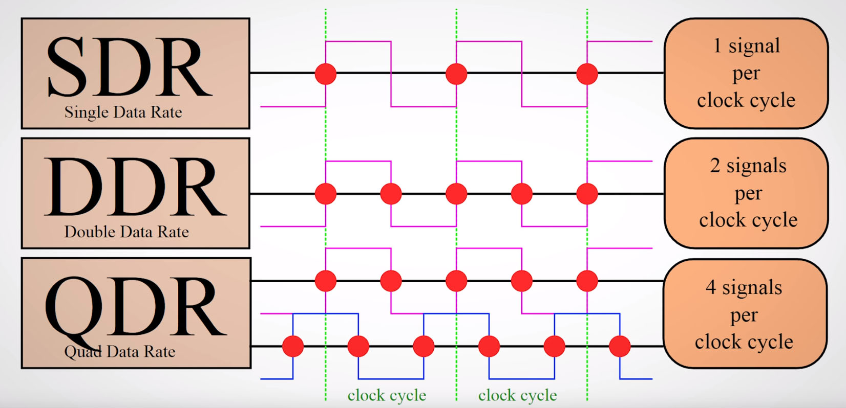
First, the basics. While memory frequency is measured in Hertz, or cycles per second, the unit for memory timings is just plain cycles. To convert clock cycles to a measurement of time requires knowing the frequency of the memory. This is listed in MHz, or units of 1,000,000Hz. 3200MHz memory has a clock frequency of 3,200,000,000 cycles per second, so the time for a cycle to complete should be (1/3,200,000,000) seconds. However, modern memory is DDR (double data rate), meaning data is transferred on the rising and falling edge of each clock, so advertised frequencies are twice the real clock frequency. That’s why when you set memory to 3200MHz in BIOS, CPU-Z will show 1600MHz. Therefore the time is really (1/(3,200,000,000/2)) seconds. If our example memory has a CL timing of 16 clock cycles, this translates to (16 * (1/(3,200,000,000/2))) seconds, or .00000001 seconds, or 10 nanoseconds.
The equation is (1/(advertised frequency/2)) * timing in cycles = timing in seconds. For a DDR3-1600 kit, a CL of 9 translates to 11.25ns, actually slower than our previous example. Latencies have gradually increased over the years with the physical distance that signals have to travel (the speed of light is a hard limit), but frequency has increased as well, and therefore performance has still improved. Frequency is very important, but it’s just one element of performance, as with CPUs.
There are many, many different timings, but they deal with a fairly small list of commands: when they can be issued, how long it takes for them to execute, how many cycles pass before a response. Here’s a table of DDR4 commands copied from Wikipedia:
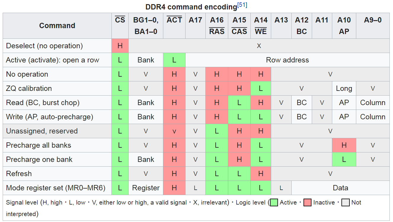
The important signals from the top row are ACT (Activate), RAS (Row Access Strobe), CAS (Column Access Strobe), and WE (Write Enable). RAS and CAS are often referred to simply as column and row address because they aren’t actually strobes; the terminology is a holdover. These are Active-Low signals, so they can be either H(igh) or L(ow), 1 or 0. Together they form a four-bit code that specifies a command to be executed. The signals have changed a bit over the years, but for the most part DDR4 has the same list of commands that SDRAM has always had, and therefore many of the same timings. For some background information on stuff like banks, rows, and columns, this venerable 2010 article from Anandtech is a good overview of what SDRAM actually is and how it functions.
For this next section, we created a custom animation that can be found in our above-embedded video. That may assist in better understanding the below definitions.
Activate: opens a row of a bank. A row must be active for reading and writing data. If a row isn’t active it’s idle, and if a row is activated it stays that way until a precharge command.
Precharge: closes the open row in one or all banks (two separate commands), putting them into the idle state. Data is still stored in idle banks, but they must be activated again before reading or writing.
Read and Write: self explanatory. With these commands, an Auto Precharge flag can be set to automatically precharge the row when done.
ZQ calibration: compensates for temperature/voltage variation. It can be a recurring command, but not frequently enough to make the related timings important to us.
Refresh: refreshes the charge in memory cells by writing data back in place without changing it. DRAM is volatile memory, which means that it requires power to store data: bits are represented by charges on capacitors, which leak over time if they aren’t read or written to. We’ll discuss this more in the next article: look for tREFI and tRFC. All banks must be idle (precharged) before a refresh.
Timings are generally divided into three categories: Primary, Secondary, and Tertiary. Primary is the broadest, the rated settings are listed on the box (e.g. 16-16-16-32 2T), and they’re usually adjustable in BIOS. Secondary are non-primary timings that can optionally be set in SPD (see next section). These include: tWR, tRFC, tRDD_L, tRDD_S, tWTR_L, tWTR_S, tRTP, tFAW, and tCWL. Their names and definitions will be covered in a future article. Tertiary is the catch-all category for everything else, and it’s a deep rabbit hole--whether or not these settings are even exposed in the BIOS varies heavily with motherboard quality, and the values vary based on individual RAM, CPU, and motherboard. We’ll be covering these further in another article.
SPD and XMP Explained
That last paragraph requires some additional explanation. Every stick of RAM contains information baked into EEPROM (Electrically Erasable Programmable Read Only Memory), including some safe timing/frequency profiles--these can be viewed in the SPD tab of CPU-Z under the JEDEC header.
The JEDEC (Joint Electron Device Engineering Council) Solid State Technology Association is an organization that publishes standards for DDR4, DDR5, SSDs, mobile memory, ESD, GDDR6, and more. They are responsible for standardizing and defining everything in this article, from abbreviations to the entire concept of DDR4. As part of this, JEDEC publishes tables of baseline timings for different RAM types, several of which are saved in SPD. Memory manufacturers technically produce strictly JEDEC-defined varieties of RAM, like DDR3 1600MHz 11-11-11-28, but can make them capable of higher speeds and market them as such. For example, Corsair sells 4600MHz memory, which as of this writing is a higher speed than JEDEC has defined for DDR4. When a newly-built system is powered on for the first time, the board will check SPD and default to the best set of these JEDEC approved slow-but-safe speeds.
XMP is an SPD extension. XMP, or eXtreme Memory Profiles, are higher-performance specs jammed into the leftover space in the EEPROM. These are conceptually the same thing as the JEDEC profiles, but they’re optimized by the memory manufacturer. XMP contains settings that the memory manufacturer says will probably work, but may not be supported depending on the quality of the CPU IMC or SOC and other components. For enthusiast RAM, the advertised speeds are usually only attainable by applying XMP.
XMP is technically an Intel term and an Intel standard, but an “extreme memory profile” is literally just a list of numbers that can be read by any system (if the board allows it). For example, DOCP and EOCP on AMD boards are just generic names for XMP. “XMP Profile” is redundant, but just remember: nobody cares, including Intel, or they’d have abbreviated “extreme” correctly.
Neither SPD nor XMP contains every timing. According to a Kingston representative: “We tune the ‘Primary’ timings (CL,RCD,RP,RAS) only. Other timings are left alone at JEDEC’s recommendations, likely for the MRC.” In regards to some specific subtimings we asked about, “since they are not in the SPD (or XMP), we can’t change them even if we need to.” This lines-up with our experiences in the “Real World Impact” section of this article. Even if memory manufacturers wanted to go deeper, there is a specific and limited list of SPD entries.
If you’re reading these articles because you want to know whether to tune memory, the answer for most mainstream users is “no, definitely not.” We’ve done a lot of memory tuning for our #RIPLTT streams, and it can take a day (or more) to dial-in optimal timings -- and even those might have occasional memory errors. Enabling XMP and calling it a day generally does a good enough job. Memory tuning is the domain of overclockers, hardware enthusiasts, and people with a lot of time on their hands, but it’s not worth it for users who just want something with low effort requirements. XMP will cover that camp.
What Is Memory Training & How to Train Memory?
So, when it comes down to it, RAM doesn’t set its own frequency and timings--the BIOS does, with SPD/XMP as a starting point. On Intel boards, this element of the BIOS is called the MRC. This is one area where board manufacturers can secure an advantage in performance, because the sheer variety of RAM and the differences between Samsung, Micron, and Hynix chips make tertiary timings hideously complex to adjust. Memory and board manufacturers can work together to bake-in optimal timings for popular kits, but for the most part these are determined (if left on auto) during POST, where they should remain unchanged unless there are boot failures.
Memory training can appear as a black art to casual overclockers, where RAM can be magically “broken in” by repeatedly forcing boot failures until an unstable OC becomes stable enough for benchmarks. What’s actually happening is that the IMC will try a variety of settings in an attempt to stabilize the system (not all of them timings). On the user end, it can feel like trying to solve a jigsaw puzzle by shaking the box, but it works. This is an important point even for non-overclockers: if memory isn’t stable with XMP, allow the system to reboot a few times before giving up.
Real-World Impact of Lower Level Memory Timings
Different kits have different JEDEC standards, so different subtimings get loaded. This is an issue we’ve run into before: we had two kits identical in frequency and capacity, but with different latencies; however, the 16-18-18-36 Corsair kit somehow outperformed the 14-14-14-34 G.SKILL kit in tests. After discussing this with both manufacturers, it turned out that Corsair’s sticks were dual-sided with groups of 512MBx8 ICs (memory chips), while G.SKILL’s were single-sided with groups of 1GBx8 ICs.
512MBx8 is an older style, so it actually has tighter subtimings defined by JEDEC (see “What Are Timings?”). The biggest culprit in this case was tRFC, or Refresh Cycle Time. We’ll cover the full definition of this in part 2, but for now the important thing is that the value set by JEDEC for Corsair’s type of kit was 416 and 560 for G.SKILL’s. When we adjusted the G.SKILL kit’s tRFC value down to match Corsair’s with no other adjustments, it pulled ahead in performance and remained stable, as shown in the Ashes of the Singularity results below:
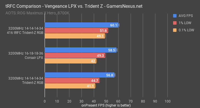
This is an extreme case, but it shows both the value of experimenting with subtimings and the frustrations of benchmarking memory. If the ASUS board had happened to have a set of optimized timings for this specific G.SKILL kit, it would have performed better than the Corsair kit from the start.
Primary Timings: tCL/tCAS, tRCD, tRP, & tRAS Explained
With all that out of the way, it’s time to talk about the primary set of timings. On any product listing, box, or stick of RAM, timings will be listed in the format tCL-tRCD-tRP-tRAS, with CR sometimes listed as well.
CAS Latency (tCL/tCAS):
Wikipedia: “The number of cycles between sending a column address to the memory and the beginning of the data in response. This is the number of cycles it takes to read the first bit of memory from a DRAM with the correct row already open. Unlike the other numbers, this is not a maximum, but an exact number that must be agreed on between the memory controller and the memory.”
CAS Latency is the most widely talked about and compared memory timing. The CL timing is an exact number, the base time that it takes to get a response from memory in the best possible scenario described above, referred to as a “page hit.” The other primary timings (other than command rate) are minimums. It’s important to remember that although we’ll be talking about how these timings relate to reading data from memory, that’s just one thing they affect.
RAS to CAS Delay (tRCD):
Wikipedia: “The minimum number of clock cycles required between opening a row of memory and accessing columns within it. The time to read the first bit of memory from a DRAM without an active row is tRCD + CL.”
RAS to CAS is one potential delay to read/writes. tRCD is the number of clock cycles it takes to open a row and access a column. If a request for data is made when there are no rows open, referred to as “page miss,” it will take at least tRCD + CL clock cycles for the CPU to receive the first bit of data in response.
Row Precharge Time (tRP):
Wikipedia: “The minimum number of clock cycles required between issuing the precharge command and opening the next row. The time to read the first bit of memory from a DRAM with the wrong row open is tRP + tRCD + CL.”
If the wrong row is open (“page miss”), it needs to be closed (precharged), then the next needs to be opened, then the column within the row needs to be accessed. This therefore takes tRP + tRCD + CL time.
Row Active Time (tRAS):
Wikipedia: “The minimum number of clock cycles required between a row active command and issuing the precharge command. This is the time needed to internally refresh the row, and overlaps with tRCD. In SDRAM modules, it is simply tRCD + CL. Otherwise, approximately equal to tRCD + 2×CL.”
Also known as Activate to Precharge Delay or Minimum RAS Active Time. The first equation (for SDRAM) is the relevant one here, but it should be more than that. We’ve seen multiple different “true” ways to calculate tRAS, but given the complexity of memory operations, good old trial and error remains the easiest. For example, we somehow booted with memory at 16-16-16-26, and that doesn’t make sense by anyone’s rules.
Command Rate (CR/CMD/CPC/tCPD):
AMD: The amount of time, in cycles, between when a DRAM chip is selected and a command is executed. 2T CR can be very beneficial for stability with high memory clocks, or for 4-DIMM configurations.
Also known as Command Period. This will either be 1T or 2T on modern memory, with 1T being faster. Despite the unique -T notation, this is measured in clock cycles like the other timings. There’s generally a very small performance delta between the two options.
Conclusion of Part 1
That’s it for the basics, but there are plenty of other timings to define and explain. Check back for part 2, where we’ll explore the secondary and tertiary timings of DDR4 memory.
If any of this would be better with a visual aid, try our embedded video (above) for an animated walkthrough of how some of the memory accesses work. We’ll be back with secondary and tertiary timings soon enough.
Editorial, Research: Patrick Lathan
Host: Steve Burke
Video: Andrew Coleman