The AMD Radeon VII embargo for “unboxings” has lifted and, although we don’t participate in the marketing that is a content-filtered “unboxing,” a regular part of our box-opening process involves taking the product apart. For today, restrictions are placed on performance discussion and product review, but we are free to show the product and handle it physically. You’ll have to check back for the review, which should likely coincide with the release date of February 7.
This content is primarily video, as our tear-downs show the experience of taking the product apart (and discoveries as we go), but we’ll recap the main point of interest here. Text continues after the embedded video:
A note before starting: All of our core testing was complete prior to this tear-down, so data, especially thermal data, will be unaffected by this content. We eventually had to take it apart (video above) to do our PCB analysis and thermocouple placement on the MOSFETs.
Disassembly is easy overall. The backplate is secured with TR8 screws – slightly different in positioning and sizing from Vega 56 and Vega 64 – but is otherwise familiar. The backplate removes easily and reveals a host of PH0 screws. These route through the PCB and into the baseplate, with the usual 4 PH screws for the GPU cooler.
The cooler is a vapor chamber mixed with 10mm heatpipes, each routed over the vapor chamber (and connecting to the finstack). The heatpipes are of the flat variety, allowing greater surface area contact to the finstack and baseplate. As usual, the heatpipes are soldered to the finstack directly, and the flattened approach does increase that surface area significantly. Triple axial fans are used to cool the finstack, with the GPU+HBM vapor chamber taking care of the most thermally intensive part of the job.
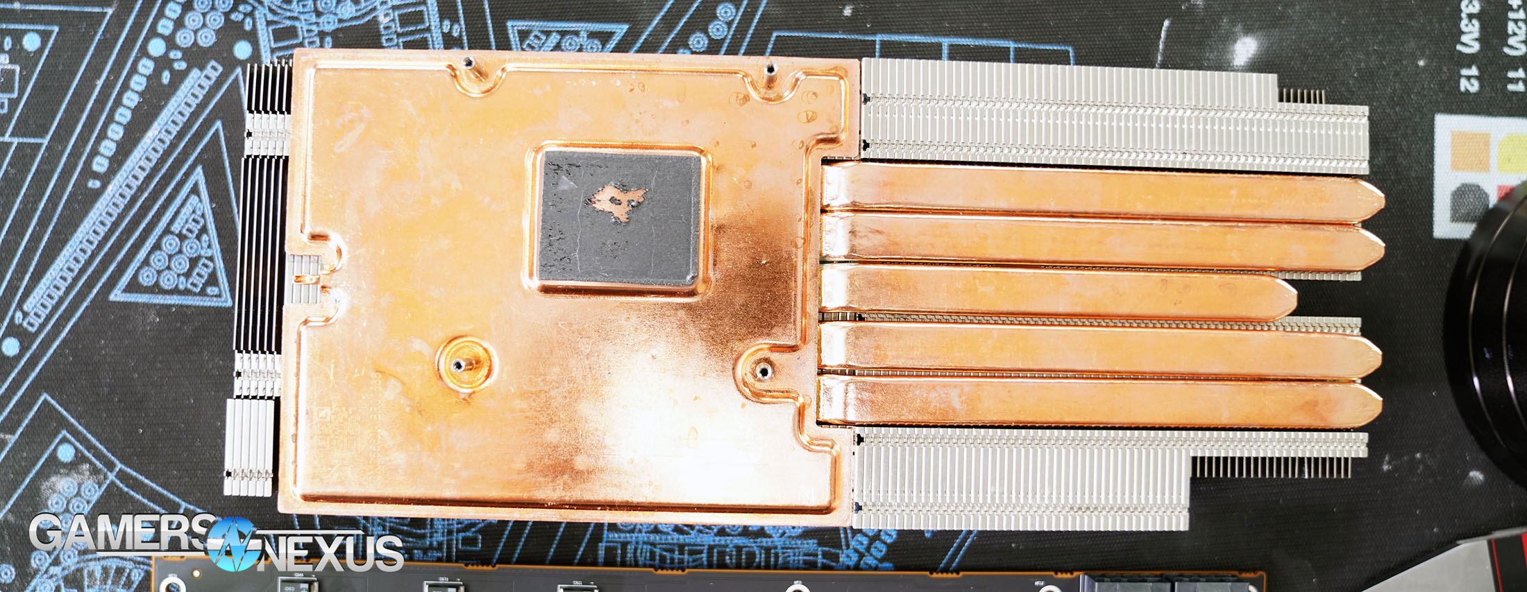
Interestingly, the thermal interface between the GPU and vapor chamber is not paste, but instead a thermal pad. AMD is using a Hitachi HM03 graphite thermal pad. The official thermal conductivity is between ~40W/mK and ~90W/mK, with the effective range closer to 25-45W/mK, although how Hitachi defines “effective” is still unclear to us. We assume it has to do with orientation. This pad would theoretically be less effective than a thinner paste, not better, as the thickness is counter-productive to thermal dissipation. We will talk about this more in the review. It does have distinct advantages, though, one of which is age, and another of which is likely resolving packaging height differences that AMD saw in its initial Vega 56 and Vega 64 die packaging. We talked about Vega mounting pressure issues here previously, and believe that this thermal pad would resolve further issues.
As for the Radeon VII card, our model uses a GPU + HBM package with an epoxy resin coating, ensuring equal height across all the dies on the interposer. We are unsure if there are packaging across other Radeon VII cards, and won’t really know until more people open theirs up. Vega 56 and Vega 64 had three different types of assembly.
We’ll leave it here for the article. Check the video above for more information and check back shortly for the review.
Editorial, Host: Steve Burke
Video: Andrew Coleman