The Titan X Hybrid mod we hand-crafted for a viewer allowed the card to stretch its boost an additional ~200MHz beyond the spec. This was done for Sam, the owner who loaned us the Titan XP, and was completed back in August. We also ran benchmarks before tearing the card down, albeit on drivers from mid-August, and never did publish a review of the card.
This content revisits the Titan XP for a review from a gaming standpoint. We'd generally recommend such a device for production workloads or CUDA-accelerated render/3D work, but that doesn't stop that the card is marketed as a top-of-the-line gaming device with GeForce branding. From that perspective, we're reviewing the GTX Titan X (Pascal) for its gaming performance versus the GTX 1080, hopefully providing a better understanding of value at each price-point. The Titan X (Pascal) card is priced at $1200 from nVidia directly.
Review content will focus on thermal, FPS, and overclocking performance of the GTX Titan X (Pascal) GP102 GPU. If you're curious to learn more about the card, our previous Titan XP Hybrid coverage can be found here:
NVIDIA Titan X (Pascal) Specs
| NVIDIA Pascal vs. Maxwell Specs Comparison | |||||||
| Titan X | GTX 1080 | GTX 1070 | GTX 1060 | GTX 980 Ti | GTX 980 | GTX 960 | |
| GPU | GP102-? Pascal | GP104-400 Pascal | GP104-200 Pascal | GP106 Pascal | GM200 Maxwell | GM204 Maxwell | GM204 |
| Transistor Count | 12B | 7.2B | 7.2B | 4.4B | 8B | 5.2B | 2.94B |
| Fab Process | 16nm FinFET | 16nm FinFET | 16nm FinFET | 16nm FinFET | 28nm | 28nm | 28nm |
| CUDA Cores | 3584 | 2560 | 1920 | 1280 | 2816 | 2048 | 1024 |
| GPCs | 6 | 4 | 3 | 2 | 6 | 4 | 2 |
| SMs | 28 | 20 | 15 | 10 | 22 | 16 | 8 |
| TPCs | 28 | 20 | 15 | 10 | - | - | - |
| TMUs | 224 | 160 | 120 | 80 | 176 | 128 | 64 |
| Core Clock | 1417MHz | 1607MHz | 1506MHz | 1506MHz | 1000MHz | 1126MHz | 1126MHz |
| Boost Clock | 1530MHz | 1733MHz | 1683MHz | 1708MHz | 1075MHz | 1216MHz | 1178MHz |
| FP32 TFLOPs | 11TFLOPs | 9TFLOPs | 6.5TFLOPs | 4.4TFLOPs | 5.63TFLOPs | 5TFLOPs | 2.4TFLOPs |
| Memory Type | GDDR5X | GDDR5X | GDDR5 | GDDR5 | GDDR5 | GDDR5 | GDDR5 |
| Memory Capacity | 12GB | 8GB | 8GB | 6GB | 6GB | 4GB | 2GB, 4GB |
| Memory Clock | 10Gbps | 10Gbps GDDR5X | 8Gbps | 8Gbps | 7Gbps GDDR5 | 7Gbps GDDR5 | 7Gbps |
| Memory Interface | 384-bit | 256-bit | 256-bit | 192-bit | 384-bit | 256-bit | 128-bit |
| Memory Bandwidth | 480GB/s | 320.32GB/s | 256GB/s | 192GB/s | 336GB/s | 224GB/s | 115GB/s |
| TDP | 250W | 180W | 150W | 120W | 250W | 165W | 120W |
| Power Connectors | 1x 8-pin 1x 6-pin | 1x 8-pin | 1x 8-pin | 1x 6-pin | 1x 8-pin 1x 6-pin | 2x 6-pin | 1x 6-pin |
| Release Date | 8/2/2016 | 5/27/2016 | 6/10/2016 | 7/19/2016 | 6/01/2015 | 9/18/2014 | 01/22/15 |
| Release Price | $1200 | Reference: $700 MSRP: $600 | Reference: $450 MSRP: $380 | Reference: $300 MSRP: $250 | $650 | $550 | $200 |
NVIDIA Titan X (Pascal) GP102 Architecture
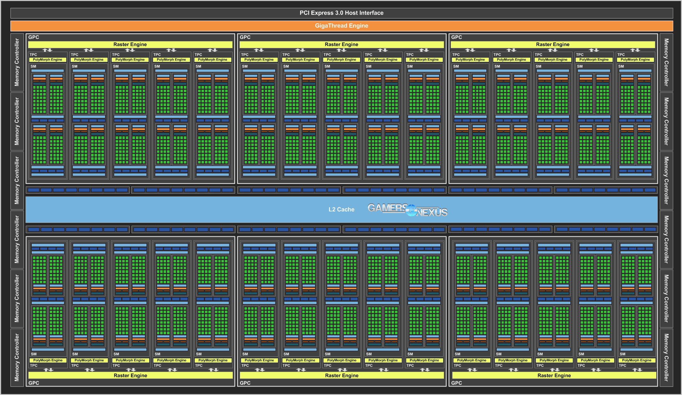
The Titan XP uses a GP102 GPU under Pascal architecture, the largest Pascal chip presently available on a GeForce-branded card. The only current Pascal chip that's equipped in a flashier fashion than the GP102 is GP100, used for the Tesla P100 Accelerator and not meant for gaming. We detailed GP100 a few months ago, if interested in learning more about Pascal's intricacies.
GP102 hosts a total of 6 GPCs, for 28 SMs and 3584 CUDA cores. This isn't the biggest Pascal chip out, in terms of total SMs, but it's the biggest in the GeForce line. GP102 follows GP104's architecture and splits GPCs into sets of 5SMs, as opposed to the GP100 GPC-SM alignment of 10 simultaneous multiprocessors per GPC. This is why we often remind folks that cores and SMs can't be compared cross-generation, or sometimes even intra-generation. The GP100 chip used for the Tesla P100 Accelerator is built for simulation and deep learning, which means it's got a completely different implementation of cores. GP100 makes use of FP64 cores in a way that the Titan XP does not, and so is more suitable for double-precision tasks than the FP32-focused Titan X card of this generation.
Also like GP104-400, the Titan XP runs 8 TMUs per SM, totaling 224 texture map units. Clock-rate natively operates at 1531MHz with the stock cooler and hits 1700MHz or higher during load. Note also that we pushed to nearly 2000MHz in our liquid content without needing to overclock – that's GPU Boost 3.0 in action. The Boost behavior has detected thermal headroom to push the clock higher, and so it increases the operating frequency until a point at which a new limiter is encountered (normally power or voltage).
Cache size also plays a big role in the Titan XP. The TiXP expands cache to 3072KB over the 2048KB on the GTX 1080. VRAM on-board is 12GB for the Titan XP, versus 8GB for the GTX 1080. Both use GDDR5X at 10Gbps native.
Titan XP and GP102 host 12 billion total transistors and, despite a focus on FP32, works to introduce a new INT8 deep-learning instruction set. We're not benchmarking that today, though.
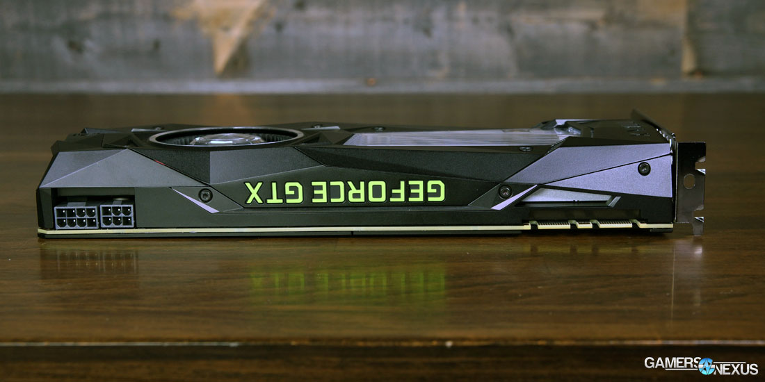
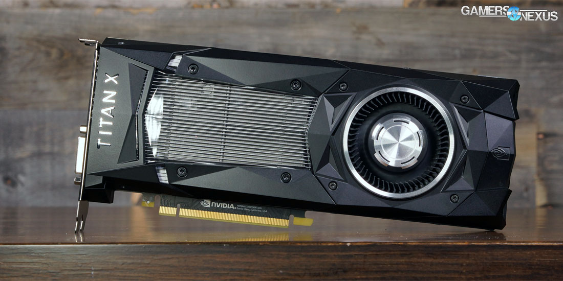
NVIDIA Titan X (Pascal) Tear-Down, PCB, & Cooler
Below are a few photos from our tear-down content:
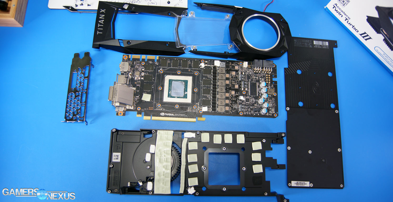
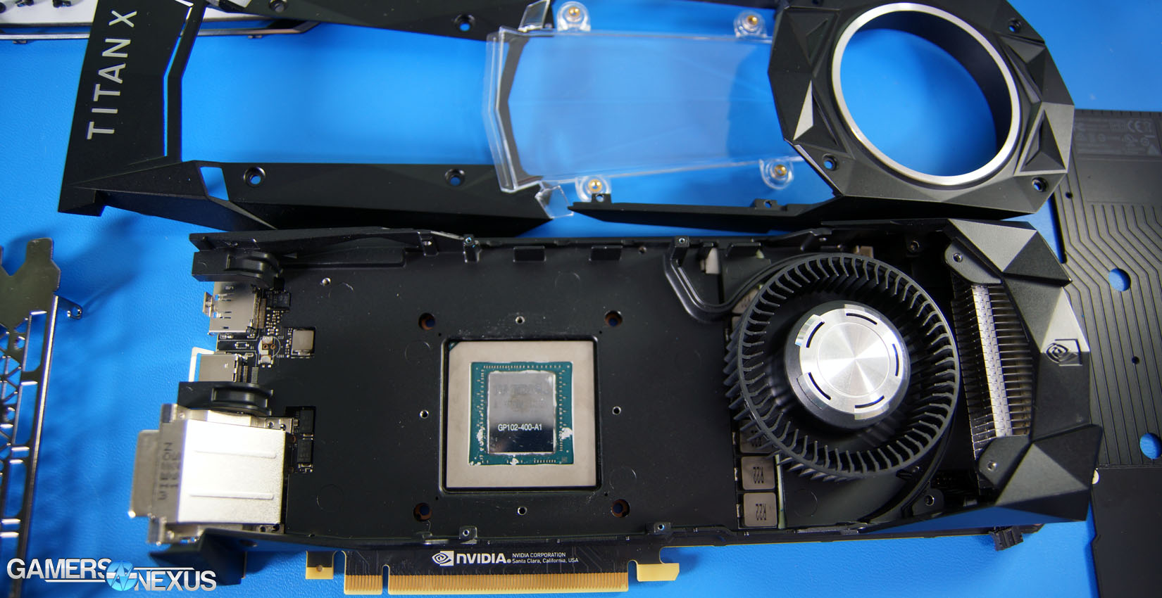
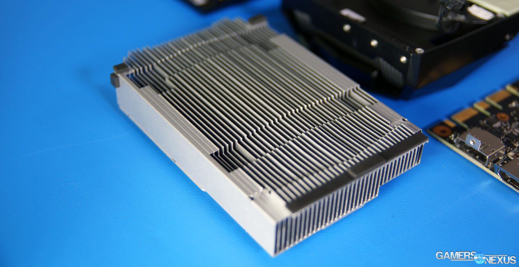
The disassembly process for the Titan XP is almost exactly the same as what is used to disassemble the GTX 1080. The card uses a vapor chamber cooler for its thermal solution, coupled with a blower fan and usual PWM control. An aluminum baseplate rests between the PCB and the faceplate, which uses thermal pads to conduct heat into the plate. Air from the blower fan then pushes air through fins atop the baseplate, dissipating heat and pulling it away from VRAM and the VRM. This air is eventually pushed through the vapor chamber cooler, then out the back of the card.
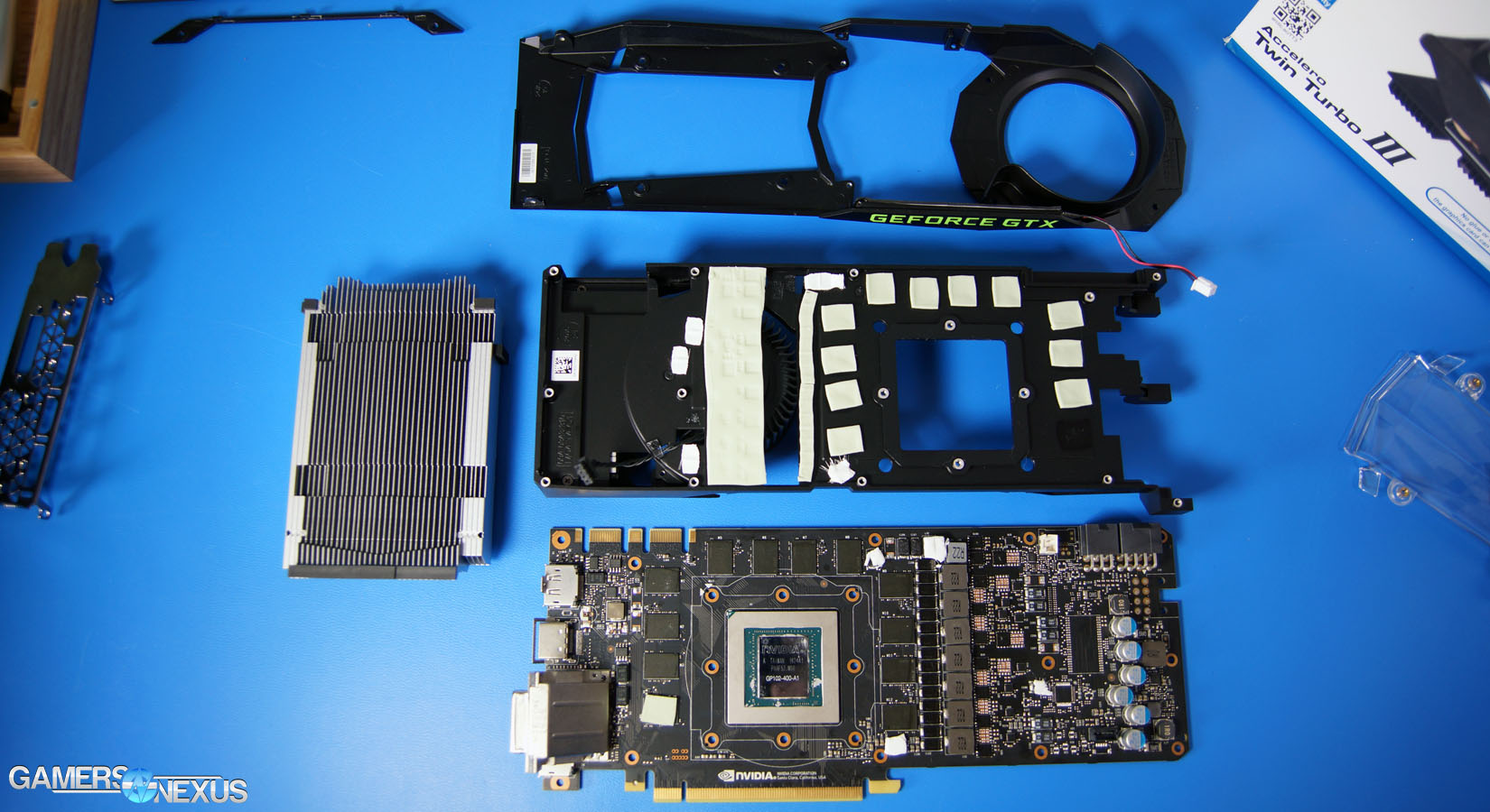
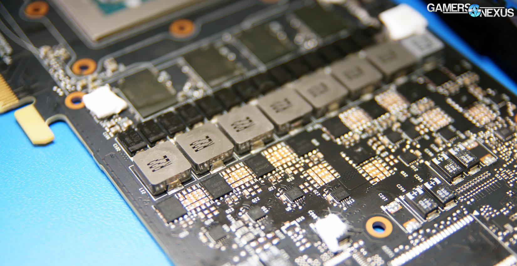
The PCB hosts two power connectors and a third set of solder points for an additional 8-pin header, located at the right side of the board. The core VRM uses a 7-phase power design, with the memory VRM using a 2-phase design.
Continue to page 2 for test methodology.
Test Methodology
Game Test Methodology
Note that all thermals, FPS, noise, and overclocking tests were performed before our initial tear-down, so the only difference you'll see in numbers emerges after we applied a liquid cooler to the Titan XP. This data was collected in August of 2016, since it was our only chance to work with the card.
We tested using our GPU test bench, detailed in the table below. Our thanks to supporting hardware vendors for supplying some of the test components.
AMD 16.8.1 drivers were used for the RX 470 & 460 graphics cards. 16.7.2 were used for testing GTA V & DOOM (incl. Vulkan patch) on the RX 480. Drivers 16.6.2 were used for all other devices or games. NVidia's 372.54 drivers were used for game (FPS) testing on the GTX 1080 and 1060 (and Titan XP). The 368.69 drivers were used for other devices. Game settings were manually controlled for the DUT. All games were run at presets defined in their respective charts. We disable brand-supported technologies in games, like The Witcher 3's HairWorks and HBAO. All other game settings are defined in respective game benchmarks, which we publish separately from GPU reviews. Our test courses, in the event manual testing is executed, are also uploaded within that content. This allows others to replicate our results by studying our bench courses.
Windows 10-64 build 10586 was used for testing.
Each game was tested for 30 seconds in an identical scenario, then repeated three times for parity.
Average FPS, 1% low, and 0.1% low times are measured. We do not measure maximum or minimum FPS results as we consider these numbers to be pure outliers. Instead, we take an average of the lowest 1% of results (1% low) to show real-world, noticeable dips; we then take an average of the lowest 0.1% of results for severe spikes.
| GN Test Bench 2015 | Name | Courtesy Of | Cost |
| Video Card | This is what we're testing! | - | - |
| CPU | Intel i7-5930K CPU | iBUYPOWER | $580 |
| Memory | Corsair Dominator 32GB 3200MHz | Corsair | $210 |
| Motherboard | EVGA X99 Classified | GamersNexus | $365 |
| Power Supply | NZXT 1200W HALE90 V2 | NZXT | $300 |
| SSD | HyperX Savage SSD | Kingston Tech. | $130 |
| Case | Top Deck Tech Station | GamersNexus | $250 |
| CPU Cooler | NZXT Kraken X41 CLC | NZXT | $110 |
For Dx12 and Vulkan API testing, we use built-in benchmark tools and rely upon log generation for our metrics. That data is reported at the engine level.
Video Cards Tested
- Corsair Hydro GFX GTX 1080 ($750)
- Sapphire RX 470 Platinum (~$180?)
- MSI RX 480 Gaming X
- MSI GTX 1060 Gaming X ($290)
- NVIDIA GTX 1060 FE ($300)
- AMD RX 480 8GB ($240)
- NVIDIA GTX 1080 Founders Edition ($700)
- NVIDIA GTX 980 Ti Reference ($650)
- NVIDIA GTX 980 Reference ($460)
- NVIDIA GTX 980 2x SLI Reference ($920)
- AMD R9 Fury X 4GB HBM ($630)
- AMD MSI R9 390X 8GB ($460)
- And more
Thermal Test Methodology
We strongly believe that our thermal testing methodology is among the best on this side of the tech-media industry. We've validated our testing methodology with thermal chambers and have proven near-perfect accuracy of results.
Conducting thermal tests requires careful measurement of temperatures in the surrounding environment. We control for ambient by constantly measuring temperatures with K-Type thermocouples and infrared readers. We then produce charts using a Delta T(emperature) over Ambient value. This value subtracts the thermo-logged ambient value from the measured diode temperatures, producing a delta report of thermals. AIDA64 is used for logging thermals of silicon components, including the GPU diode. We additionally log core utilization and frequencies to ensure all components are firing as expected. Voltage levels are measured in addition to fan speeds, frequencies, and thermals. GPU-Z is deployed for redundancy and validation against AIDA64.
All open bench fans are configured to their maximum speed and connected straight to the PSU. This ensures minimal variance when testing, as automatically controlled fan speeds will reduce reliability of benchmarking. The CPU fan is set to use a custom fan curve that was devised in-house after a series of testing. We use a custom-built open air bench that mounts the CPU radiator out of the way of the airflow channels influencing the GPU, so the CPU heat is dumped where it will have no measurable impact on GPU temperatures.
We use an AMPROBE multi-diode thermocouple reader to log ambient actively. This ambient measurement is used to monitor fluctuations and is subtracted from absolute GPU diode readings to produce a delta value. For these tests, we configured the thermocouple reader's logging interval to 1s, matching the logging interval of GPU-Z and AIDA64. Data is calculated using a custom, in-house spreadsheet and software solution.
Endurance tests are conducted for new architectures or devices of particular interest, like the GTX 1080, R9 Fury X, or GTX 980 Ti Hybrid from EVGA. These endurance tests report temperature versus frequency (sometimes versus FPS), providing a look at how cards interact in real-world gaming scenarios over extended periods of time. Because benchmarks do not inherently burn-in a card for a reasonable play period, we use this test method as a net to isolate and discover issues of thermal throttling or frequency tolerance to temperature.
Our test starts with a two-minute idle period to gauge non-gaming performance. A script automatically triggers the beginning of a GPU-intensive benchmark running MSI Kombustor – Titan Lakes for 1080s. Because we use an in-house script, we are able to perfectly execute and align our tests between passes.
Power Testing Methodology
Power consumption is measured at the system level. You can read a full power consumption guide and watt requirements here. When reading power consumption charts, do not read them as a GPU-specific requirements – this is a system-level power draw.
Power draw is measured during a FireStrike Extreme - GFX2 run. We are currently rebuilding our power benchmark.
Note that all thermals, FPS, noise, and overclocking tests were performed before our initial tear-down, so the only difference you'll see in numbers emerges after we applied a liquid cooler to the Titan XP. We've already produced that content, but will briefly revisit here.
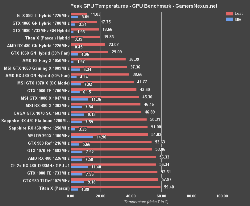
Titan X Pascal Temperature
We're keeping the thermal discussion short since it was already so heavily covered in our Hybrid GTX Titan XP mod that was already published. The results are interesting, though, and absolutely worth a watch or a read if you've not already seen them.
Recapping the basics, the reference GTX Titan X design hits its thermal limit at 83-84C GPU diode temperature, non-delta, and that's what creates the Boost specification of 1531MHz. The clock actually automatically boosts higher through GPU Boost 3.0 when that thermal limit is bypassed by superior cooling. Our Hybrid mod, for instance, brings us down to 19.85C delta T from 59.4C on the FE cooler, which uses just a vapor chamber and blower fan. That's a reduction of ~40C for the load temperature.
As for idle temperatures, those are a little lower than the 1080 for a few reasons: (1) the die size is 471mm^2 on the GP102 chip, whereas the GP104 chip is 314mm^2, and this extra surface area helps dissipate heat; (2) for liquid testing, we've improved our implementation by keeping the baseplate on the Titan X Hybrid, not done for the 1080 Hybrid. These results are for the stock Titan XP card. We've dropped thermals by 40C and increased clock-rate without overclocking on our Hybrid mod, showing clear headroom for the stock unit to boost higher with a better cooler.
This next section is an excerpt from our Hybrid results article:
Titan X Pascal Endurance Test
59.4C delta T is – the hottest on the bench, actually – and that puts the GPU Diode value in the 84-85C range. The GTX 1080 limits itself at around 83C, as we've extensively shown, and uses normal Boost 3.0 functionality to down-clock the card along the volt-frequency curve, reducing thermals by reducing performance temporarily. Once the GPU has become satisfied with its new resting temperature, it will attempt again to increase the clock-rate. This cycle repeats ad infinitum while under load, and is a normal part of GPU functionality.
What is sub-optimal, however, is heavy clock-limiting that results in drastically reduced clock-rates. Let's look at that.
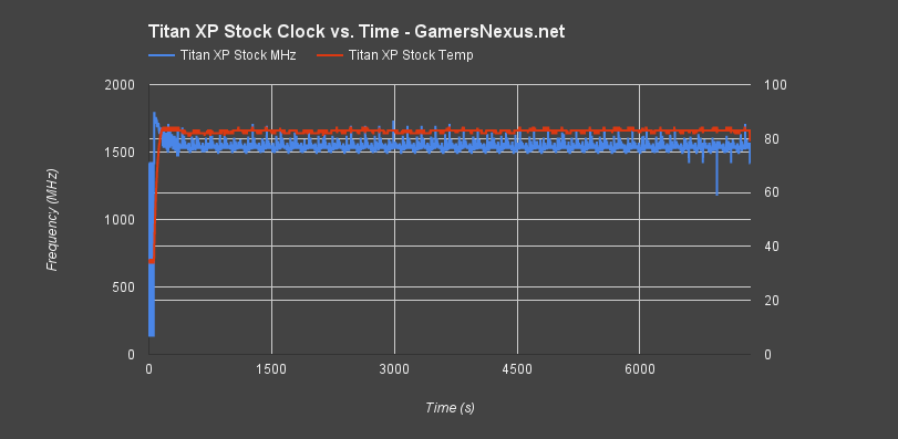
The above is an endurance chart for the stock Titan XP, before applying our liquid cooling solution.
During our endurance test, we plotted the Titan XP with its stock cooler as limiting at around 84C. Every hit to 84C caused an immediate drop in clock-rate, and the clock-rate got stuck around 1544MHz, but sometimes would spike to 1670MHz or drop as low as the 1400s. The spec calls for a 1531MHz boost, on paper, and the card mostly achieves this. The chart makes it pretty clear that our clock-rate is spiking hard, and it's a result of thermals – not power limit. We occasionally warmed to 85C or 86C, but the card mostly chokes clock-rate to keep itself at 83C. And, as we'll find in a moment, the card spec calls for well under its actual operating potential.
Here's a look at a small cross-section of raw data to show what's going on.
| Time (s) | Core MHz | GPU Diode |
| 348 | 1556.5 | 83 |
| 349 | 1556.5 | 83 |
| 350 | 1493 | 83 |
| 351 | 1531 | 84 |
| 352 | 1657.5 | 84 |
| 353 | 1645 | 84 |
| 354 | 1645 | 84 |
| 355 | 1632.5 | 84 |
| 356 | 1531 | 84 |
| 1468 | 83 |
| 358 | 1493 | 83 |
| 359 | 1544 | 84 |
| 360 | 1544 | 83 |
| 361 | 1531 | 83 |
| 362 | 1569 | 84 |
| 363 | 1531 | 84 |
| 364 | 1531 | 83 |
| 365 | 1518.5 | 83 |
| 366 | 1506 | 83 |
| 367 | 1506 | 83 |
| 368 | 1518.5 | 83 |
| 369 | 1531 | 83 |
| 370 | 1531 | 83 |
| 371 | 1531 | 83 |
| 372 | 1556.5 | 83 |
You can see that the clock has a range of more than 100MHz (in this sample of data, we've got a range of 189.5MHz, with a high of 1657.5MHz and low of 1468MHz). This clock-rate swing presents itself in 0.1% and 1% low values for gamers, but for production, it'll mostly manifest as an overall loss of efficiency and slow-down in render times. Because the card is so fast already, though, it might not be apparent that the slow-down exists – at least, not until after fixing the reference design. Then it's more obvious.
Let's put that into perspective.
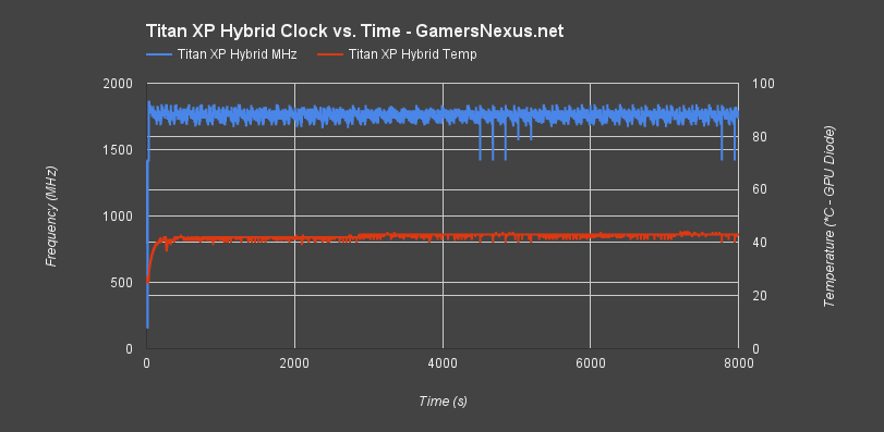
| Time (s) | Core MHz | GPU Diode (C) |
| 349 | 1771.5 | 41 |
| 350 | 1759 | 41 |
| 351 | 1784.5 | 41 |
| 352 | 1759 | 41 |
| 353 | 1759 | 41 |
| 354 | 1721 | 41 |
| 355 | 1759 | 41 |
| 356 | 1784.5 | 41 |
| 357 | 1771.5 | 41 |
| 358 | 1721 | 41 |
| 359 | 1733.5 | 41 |
| 360 | 1759 | 41 |
| 361 | 1721 | 41 |
| 362 | 1759 | 41 |
| 363 | 1721 | 41 |
| 364 | 1746.5 | 41 |
| 365 | 1721 | 41 |
| 366 | 1721 | 41 |
| 367 | 1721 | 41 |
| 368 | 1733.5 | 41 |
| 369 | 1721 | 41 |
| 370 | 1721 | 41 |
| 371 | 1695.5 | 40 |
| 372 | 1695.5 | 41 |
| 373 | 1695.5 | 41 |
(Above table: Some raw data from the Hybrid endurance run).
So, the original chart plots us as hovering in the 1468-1657+ range with an 83-84C diode, averaging at around 1531MHz. With our Hybrid mod, we brought the Titan X Pascal up to nearly 1800MHz – and that's with absolutely no overclock at all. Again, this is running stock, which means that the card's spec sheet is under its actual potential performance, and that the cooler is “stealing” speed from the chip. On average, we're moving from 1531MHz with the stock cooler to an average of about 1784MHz with the liquid cooler. We've improved the clock-rate of the stock card by more than 200MHz just by fixing nVidia's poorly performing air cooler.
The only reason we're still seeing that spiky frequency plot is because the card is now choking on power, not thermals. We've resolved the thermal constraint and are now hitting power constraints, which can be resolved simply by increasing the power limit of the card. Of course, applying an OC will re-create the spiked performance, but fixing the cooler and increasing the power limit (with no OC) will flatten overall clock-rate.
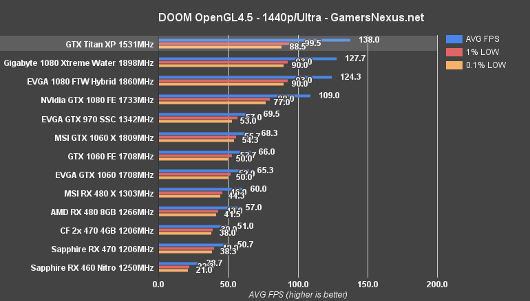
DOOM Benchmark - Titan X Pascal vs. GTX 1080
We test DOOM with both OpenGL 4.5 and Vulkan, the latter of which is presented as an average in comparative charts. Let's start just with OpenGL results.
At 1440p with Ultra settings, the Titan XP is posting an AVG FPS of 138, coupled with nearly 100FPS 1% low and about 89FPS 0.1% lows. The Gigabyte GTX 1080 Xtreme Water Force card is next in line, at about 128FPS AVG and similar lows. It's not until we get to the GTX 1080 FE that there's a reasonable gap – created almost entirely by the clock-rate difference between all the cards – where the 1080 FE pushes 109FPS AVG.
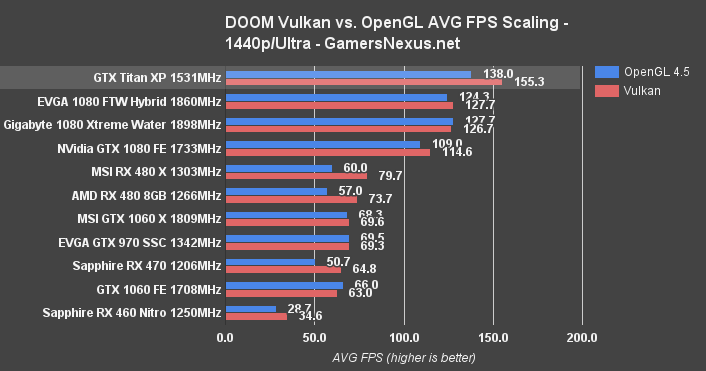
For Vulkan at 1440p, the comparison shows an FPS output of 155 AVG for the Titan XP, followed by a GTX 1080 at about 128FPS. That's a performance difference of roughly 21%, or 35% for the FE variant. We need to tax the cards a little harder to show any visible degradation in performance, though.
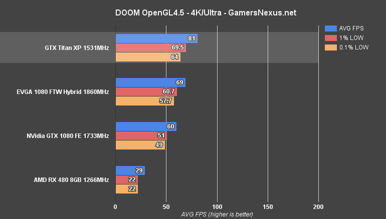
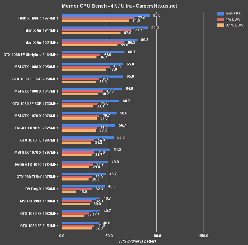
At 4K with OpenGL only, we've only got a few cards present on the bench. The GTX Titan XP pushes an AVG FPS of 81, with lows north of 60FPS. The GTX 1080 reference card is performing at 60FPS AVG, with 51FPS 1% low and 49FPS 0.1% low metrics.
Vulkan posts the Titan XP and GTX 1080 at roughly the same performance output, since we're becoming bound by the resolution.
Ashes of the Singularity - Titan XP at 4K/High
Ashes will soon be shown the door on our benchmarks, as the emergence of Battlefield 1 and Gears of War 4 have created more popular DirectX 12 options for benchmarking. It's still here for now, though, as a mainstay title that executes the new APIs with greater dexterity than some of its peers.
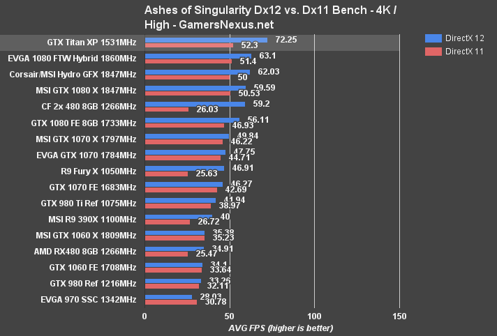
Here's a look at the FPS split between Dx12 and Dx11 at 4K High. The Titan XP gets capped in DirectX 11, as demonstrated by the proximity of the GTX 1080 FTW performance, but is granted more rope in Dx12.
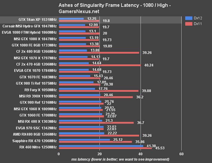
Here's the average frametime output at 10808p/high with each device on the bench, just as a point of reference. We're looking at AVG frametimes of ~12.3ms on the Titan XP and ~13 on the GTX 1080 cards, placing both within a 16ms refresh cycle for V-sync users on 60Hz displays. Dx11, however, puts us nearing 20ms, and so we'd see the occasional stutter with the older API.
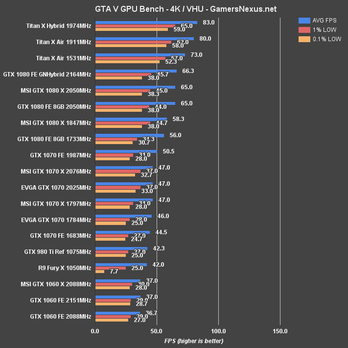
GTA V 4K Benchmark - Titan X Pascal vs. SLI GTX 1070s, GTX 1080
We tested GTA V at 4K with Very High & Ultra settings, but threw in a 1080p test just to demonstrate a point: At 1080p, we're clearly hitting a CPU bottleneck that's limiting GPU performance. The Titan XP is operating at 136FPS AVG with 95 and 85FPS 1% and 0.1% lows, respectively, which is trailed just barely by the GTX 1080 suite. If you've got plans to buy either device, it's probably worthwhile to invest in a higher resolution screen.
Performance is only limited in this fashion because we've saturated the CPU to the point that it can no longer keep up with the GPU, and so the GPU is operating at less than 100% of its full load potential. This happens most frequently with draw calls (requests for primitives/polys), as the CPU must also do work for every new frame produced. The GPU is not the only device driving high framerates.
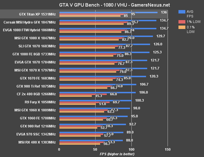
That point made, let's move on to 4K testing. The GTX Titan X is outclassed by SLI GTX 1070s in this benchmark, which jointly post a 79FPS AVG against the Titan X's 73FPS AVG. The single Titan X, as is often the case with single vs. multi-GPU configurations, outputs better frametimes than the SLI cards. Even still, the performance metrics are high enough on each device to be more or less identical with regard to user perception of framerate throughput. The difference between the configurations is about 8%, for reference, with a significant price difference. That said, there's not always good (or even positive) scaling for multi-GPU setups.
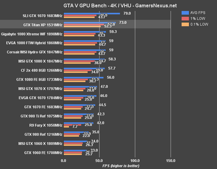
The GTX 1080 AIB partner cards operate around 59FPS AVG, or a gap of approximately 23% from the GeForce Titan X. Below these, the CrossFire RX 480s rest at 58FPS AVG, with the GTX 1080 FE is at 56FPS AVG.
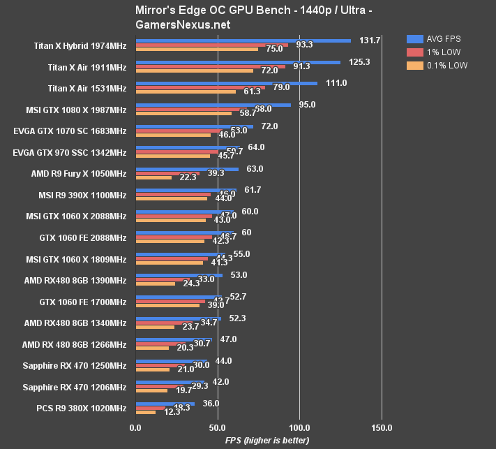
Mirror's Edge Catalyst Benchmark - GTX Titan X vs. GTX 1080
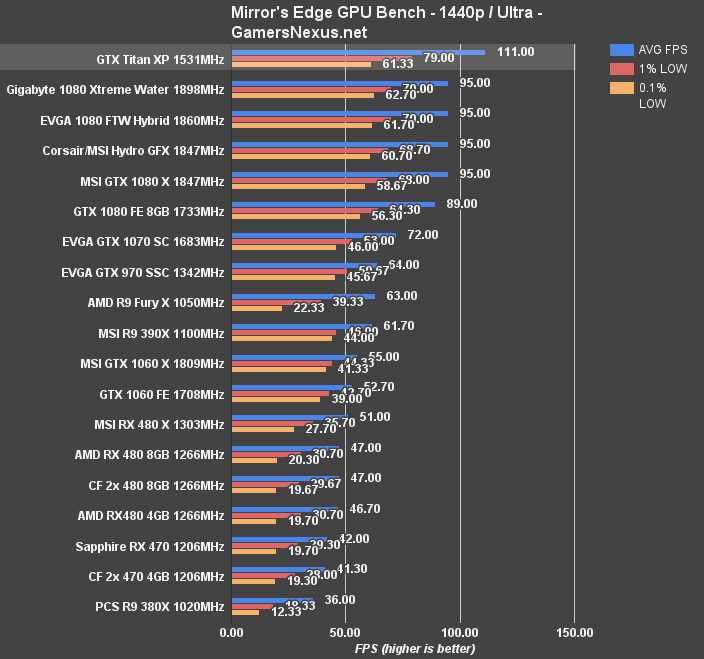
Moving on to Mirror's Edge: Catalyst at 1440p, stock Titan XP performance runs at approximately 111FPS AVG, with low framerates reasonably timed to the average and constantly above 60FPS. The Gigabyte GTX 1080 Xtreme Water Force ($770) card we reviewed, along with all the other GTX 1080s, rests at 95FPS AVG. The reference GTX 1080 operates at 89FPS AVG, or about 24% slower than the Titan XP reference card.
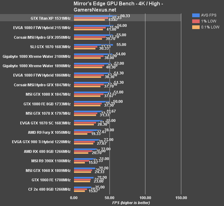
Moving to 4K, the Titan X (Pascal) card is able to sustain High quality settings at 3840x2160 with an FPS of 60.3 AVG, about 4-5FPS ahead of the liquid-cooled GTX 1080 GPUs. This framerate also places the Titan XP ~5FPS ahead of the SLI GTX 1070s. The Sea Hawk and 1080 Gaming X both run at around 51FPS AVG, with the 1070 Gaming X way down at 40.67FPS AVG and 30FPS lows.
Call of Duty: Black Ops III Benchmark - GTX Titan X vs. SLI 1070s, GTX 1080
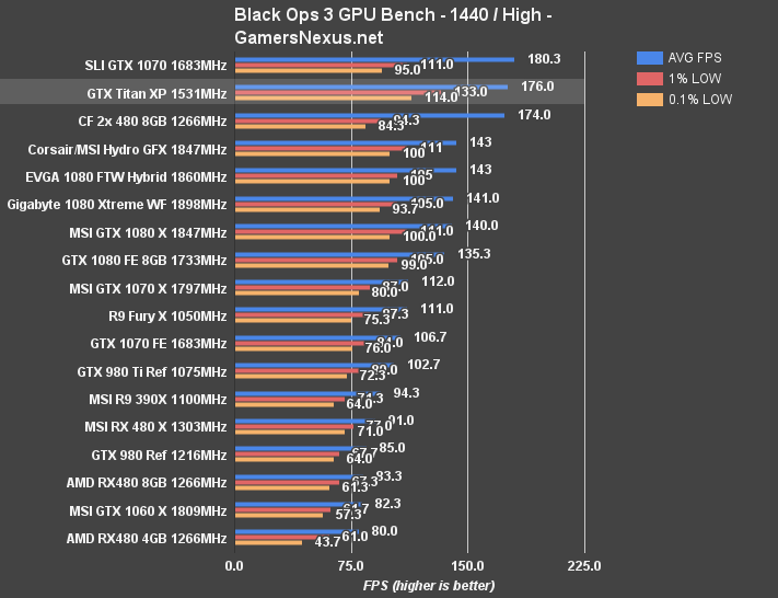
Following its performance optimization patch closer to the title's launch, Call of Duty: Black Ops III has remained one of the best-optimized titles on our benchmark. The Titan X Pascal card lands behind the SLI GTX 1070s on our bench, trailing by 4FPS in average FPS. This is sort of a moot point at this high of a framerate, but the Titan XP does hold tighter frametime performance (less latency with a single GPU -- communication is simplified) than the dual GTX 1070s. Either way, considering the price difference, we'd take the slight hit to frametimes in favor of a cheaper, similarly-paced solution. That's not always going to be the case, but it is with BLOPS3. Again, in games where SLI doesn't scale or doesn't scale well, you end up with effectively one GTX 1070 -- a far cry from the performance of a GTX Titan X.
As for single card performance at 1440p, the GTX 1080 cards land closer to ~143FPS, or about 40FPS slower than the GTX Titan X (a percentage change of ~26%).
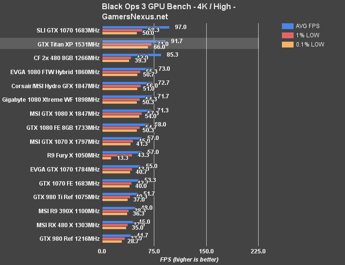
The stack remains similar at 4K, with the GTX Titan XP at ~92FPS AVG, sandwiched between the RX 480s in CrossFire (BLOPS3 does tend to favor AMD) and GTX 1070s in SLI. The GTX 1080 cards, led by the FTW Hybrid at 73FPS, tend to trail the Titan XP again by about 26%.
Metro: Last Light Benchmark - 1080p, 1440p, & 4K on Titan X Pascal
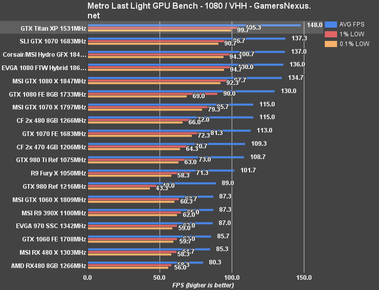
Metro: Last Light does become a bit bound by CPU at 1080p with Very High quality and High tessellation, but we're still showing some data to better illustrate the stack-up.
Let's move to something more reasonable.
MLL is another of the better-optimized titles for multi-GPU scaling, and thus plants the GTX 1070s in SLI a few frames ahead of the Titan XP's average FPS. As with previous tests, the Titan XP manages to output tighter frametimes -- again, expected, as we're running a simplified pipeline with only one GPU -- but is otherwise comparable to SLI 1070 performance.
The GTX 1080s follow, led by the 1080 Sea Hawk/Hydro GFX & FTW Hybrid at ~97FPS AVG. That's a performance gap of approximately 16%, a good deal smaller than what we saw with BLOPS3.
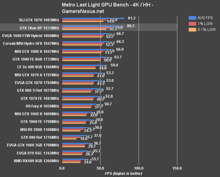
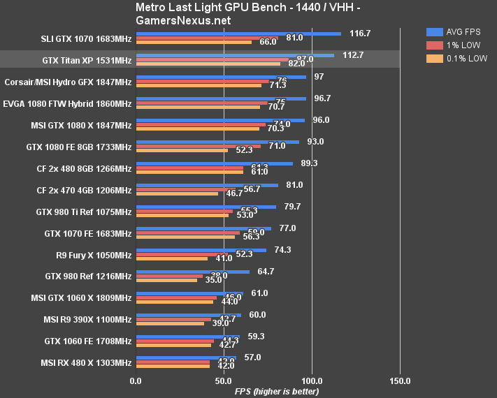
Performance tightens at 4K, with the SLI 1070s now only 1 frame ahead of the Titan XP's average. The GTX 1080 FTW Hybrid sits at ~67FPS AVG, 13FPS behind the Titan XP, creating a percentage change of 20%. The Titan XP is handling the high demand of Metro: Last Light's UHD resolution output with greater grace than the 1080 FTW Hybrid, though both remain fully "playable" and north of the 60FPS marker. Given the price disparity, that is an important point to tally.
The Division Benchmark - Titan XP vs. GTX 1080
We've axed The Division from our bench going forward, but it gets one last hurrah with the Titan XP review.
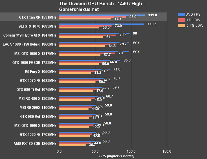
The Division operates at ~120FPS AVG on the Titan XP with 1440p/High settings, followed next by the SLI GTX 1070s at about 1FPS behind. The GTX 1080 is next, at 98FPS, followed then by the Fury X at 71FPS AVG. There's about a 20FPS performance gap between the Titan XP and GTX 1080, or ~21%.
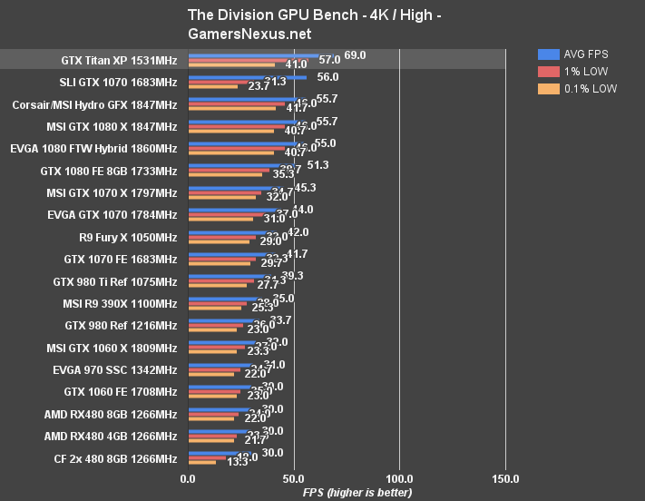
The performance distribution at 4K follows what we saw in Metro: Last Light, where the SLI 1070 cards begin to fall further behind the Titan XP on grounds of pure pixel processing power. The GTX Titan XP is now at 69FPS AVG and has 0.1% lows sustained at 41FPS, followed very distantly by 0.1% lows (perceived as stutters, in this case) of 23.7FPS on the 1070s in SLI.
NVidia's GTX 1080, as improved by the Corsair, MSI, and EVGA models on the bench, operates at around 55FPS AVG, or a difference of ~13-14FPS.
GTX Titan XP Overclocking Results
Below is our overclock stepping table with the GTX Titan XP card. With a maxed-out power target and no core offset, the average clock-rate operates at about 100MHz higher than stock with a 100% target – but we're still thermally limited. Regardless, the maximum stable overclock landed around 1911MHz average frequency, with a 175MHz offset to core and 450MHz offset to memory. The peak clock-rate was 1923.5MHz, however brief. This was with a 3500RPM fan speed, so noise levels are getting a bit more significant.
The liquid-cooled variant, for the curious, was able to sustain a maximum overclock of 2012MHz, or 1974MHz average.
| Peak Core CLK | Core Clock (MHz) | Core Offset (MHz) | Mem CLK (MHz) | Mem Offset (MHz) | Power Target (%) | Peak vCore | Fan Target (%) | 5m Test | 60m Endurance |
| 1695.5 | ~1620 | 0 | 1251.5 | 0 | 100 | 0.95 | 50 | P | P |
| 1746.5 | 1733.5 | 0 | 1251.5 | 0 | 120 | 1.025 | 65 | P | P |
| 1822.5 | 1809.5 | 100 | 1251.5 | 0 | 120 | 1.025 | 65 | P | - |
| 1860 | 1835 | 125 | 1251.5 | 0 | 120 | 1.025 | 65 | P | P |
| 1873 | 1847.5 | 150 | 1251.5 | 0 | 120 | 1.025 | 66 | P | - |
| 1923.5 | 1911 | 175 | 1251.5 | 0 | 120 | 1.025 | 66 | P | - |
| 1923.5 | 1911 | 175 | 1325.5 | 300 | 120 | 1.025 | 66 | P | - |
| 1923.5 | 1911 | 175 | 1377 | 500 | 120 | 1.025 | 66 | P | - |
| 1923.5 | 1911 | 175 | 1400.6 | 600 | 120 | 1.025 | 66 | F Driver Crash | - |
| 1987 | 1911 | 175 | 1363.5 | 450 | 120 | 1.025 | 70 | P | P |
| - | - | 200 | 1363.5 | 450 | 120 | 1.025 | 70 | F Driver Crash | - |
Hybrid mod:
| Peak Core CLK | Core Clock (MHz) | Core Offset (MHz) | Mem CLK (MHz) | Mem Offset (MHz) | Power Target (%) | Peak vCore | Fan target | 5m Test | 60m Endurance |
| 1987 | 1923.5 | 175 | 1363.5 | 450 | 120 | 1.031 | 23 (Auto) | P | P |
| 1987 | 1936 | 200 | 1363.5 | 450 | 120 | 1.031 | 23 (Auto) | P | - |
| 1999.5 | 1961.5 | 225 | 1363.5 | 450 | 120 | 1.031 | 23 (Auto) | P | - |
| 2012 | 1974 | 250 | 1363.5 | 450 | 120 | 1.031 | 23 (Auto) | P | - |
| 2037.5 | 1999.5 | 275 | 1363.5 | 450 | 120 | 1.031 | 23 (Auto) | F | - |
| 2012 | 1974 | 250 | 1363.5 | 500 | 120 | 1.031 | 23 (Auto) | P | P |
| 2012 | 1974 | 250 | 1363.5 | 600 | 120 | 1.031 | 23 (Auto) | P | P (Worse FPS) |
| 2012 | 1974 | 250 | 1363.5 | 450 | 120 | 1.031 | 23 (Auto) | P | P |
Here's a quick look at overclocking performance. We're seeing fairly substantial gains in some titles, nearing 10FPS in GTA V and Mirror's Edge Catalyst.
Continue to page 6 for the conclusion.
Titan X (Pascal) Review Conclusion
Just to sort of re-iterate the Hybrid research content, nVidia is operating at spec for its clock-rate, but the spec could actually be higher with a superior cooler. Just changing to a liquid cooler increased our average FPS by about 3.5% to 5%, depending on the title – and that's with no overclock. It feels almost wasteful to use the reference cooler on the GTX Titan X, and with a limited supply of AIB partner variants, that's going to be the most common model.
The Titan XP is still priced north of $1000, for the most part, with the GTX 1080 resting closer to $700. In its absolute best performing scenarios, the Titan XP is able to outperform a GTX 1080 FE by roughly 30%, and posts best-case gains over AIB partner 1080s upwards of 25%. But we've got to keep the bigger picture in mind: A GTX 1080 is already capable of running almost every game we've tested at 4K with roughly 60FPS framerates. For most enthusiasts at the high-end, we'd wager that's enough.
An extra $300 doesn't gain a tangible framerate improvement at this point, since we're already so high in FPS output at 1440p and in some 4K scenarios. For the most part, the GTX 1080 makes more sense as a top-of-the-line gaming card.
The Titan XP may make more sense for render and CUDA accelerated applications, once more fully support the Pascal architecture. The extra VRAM is the biggest differentiator and will stretch its legs more thoroughly in animation and CUDA-accelerated renders.
Editorial, Test Lead: Steve “Lelldorianx” Burke
Test Technician: Andie “Draguelian” Burke
Video Producer: Andrew “ColossalCake” Coleman